
Yoodli, an AI-powered communication training startup, has reached a valuation of more than $300 million — more than triple its level six months ago — as it builds technology meant to assist people rather than replace them with machines.
The valuation increase follows Yoodli’s $40 million Series B round, led by WestBridge Capital with participation from Neotribe and Madrona. It comes after a $13.7 million Series A round announced in May, bringing the startup’s total funding to nearly $60 million.
As AI tools spread into workplaces and fuel fears of automation, Yoodli positions itself differently. The four-year-old, Seattle-based startup uses AI to run simulated scenarios — including sales calls, leadership coaching, interviews, and feedback sessions — and provides users with structured, repeatable practice to improve their speaking skills.
Varun Puri (pictured above, right), who previously worked at Google’s X division and handled special projects for Sergey Brin, co-founded Yoodli with former Apple engineer Esha Joshi (pictured above, left) in 2021. He became aware of communication challenges after moving to the U.S. at 18 and seeing how difficulty expressing ideas or speaking confidently affected students and young professionals from countries such as India — himself included — Puri said in an interview.
Initially, Yoodli was meant to help people practice public speaking — a skill two out of three people struggle with, Puri told TechCrunch, citing internal data. However, the startup soon saw users turning to the platform for interview preparation, sales pitches, and difficult conversations. That shift pushed Yoodli from a consumer-focused product to enterprise training, and it now offers AI role-plays and experiential learning tools for go-to-market enablement, partner certification, and management coaching.
“In the old world, companies would be training people using static, long-form content or passive videos that we’d all watch at 4x-5x speed, just to get the thing done,” said Puri. “But that doesn’t actually mean you’ve learned it.”
Companies including Google, Snowflake, Databricks, RingCentral, and Sandler Sales use Yoodli for employee or partner training. The startup also sells its platform to coaching firms such as Franklin Covey and LHH, which can tailor the system to their own methodology and training frameworks, Puri stated. He added that the tool is not designed to replace human coaches but to keep a human in the loop delivering personalized guidance.
Techcrunch event
San Francisco
|
October 13-15, 2026
“I philosophically believe that AI can get you, let’s call it from a zero to an eight or a zero to nine,” said Puri. “But the pure essence of who you are and how you show up, and your authenticity and vulnerability that a human gives you feedback on will always exist.”
The platform works with multiple large language models, meaning users can run it with models such as Google’s Gemini or OpenAI’s GPT based on their preference. Enterprises can also embed it into their existing software, or users can access it directly through a web browser. The AI supports most major languages, including Korean, Japanese, French, Canadian French, and a list of Indian languages.
Yoodli does not offer a dedicated mobile app, a decision Puri said was made to avoid adding extra steps for users during training sessions.

Puri did not disclose how many people use the platform but said most of Yoodli’s revenue now comes from enterprise customers. He added that between the Series A and B rounds, Yoodli saw a 50% increase in the number of role-plays run on the platform and in the total time users spent practicing. The startup also said it grew its average recurring revenue by 900% over the last 12 months, though it did not provide specific figures.
Yoodli had not planned to raise more funding so soon after its last round but saw unanticipated investor interest, with WestBridge leading the latest raise, Puri said. He noted that strong performance metrics, key customers, and senior hires helped attract investors. The startup has recently hired former Tableau and Salesforce executive Josh Vitello as chief revenue officer (CRO), former Remitly CFO Andy Larson as CFO, and former Tableau chief product officer (CPO) Padmashree Koneti as CPO.
Yoodli is not alone in the market for AI-based communication tools, but Puri told TechCrunch the startup differentiates itself through deep customization and a focus on specific training verticals, allowing companies to tailor the system to their use cases and coaching methods.
The Seattle-headquartered startup has about 40 employees. Puri said the latest funding will be used to expand Yoodli’s AI coaching, analytics, and personalization tools, and to grow its presence in enterprise learning and professional development. The company also plans to hire across product, AI research, and customer success, and to expand into markets in the Asia-Pacific region while deepening its footprint in the U.S.
Source link
#ExGooglers #Yoodli #triples #valuation #300M #built #assist #replace #people #TechCrunch


![IBM Crosses One of Computing’s Biggest Barriers With World’s First Sub-1 Nanometer Chip
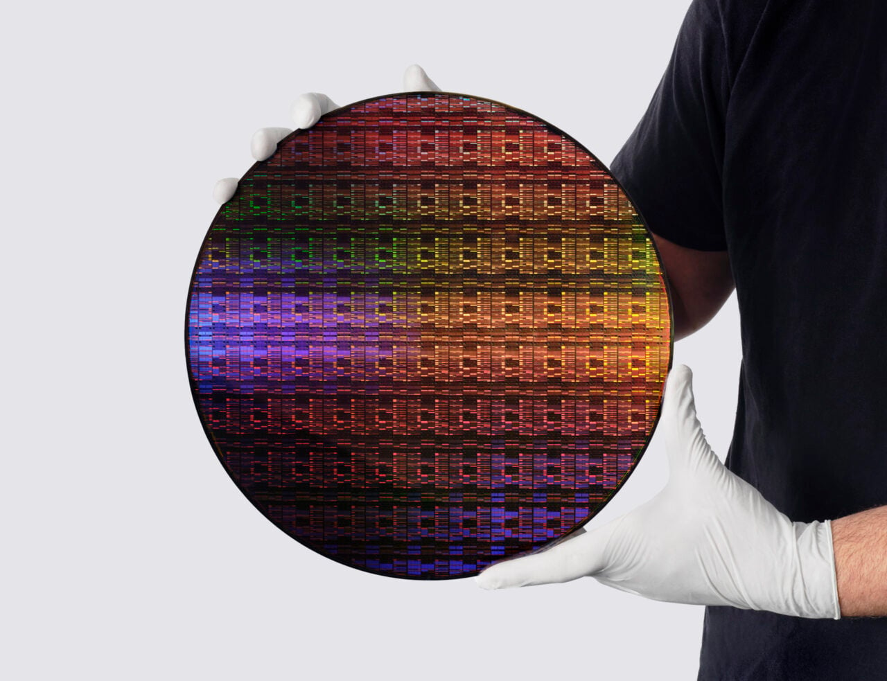
In a major breakthrough, IBM revealed the world’s first semiconductor chip technology built on a sub-1 nanometer chipmaking process. For comparison, the process uses transistor features smaller than the width of a DNA strand, which measures about 2.5 nanometers across. The chip itself is about the size of a fingernail but holds almost 100 billion transistors, and the company expects it could enter markets as early as the next five years. In a statement released today, IBM said the new chip features nearly twice the density of its 2-nanometer chip, released in 2021. According to an accompanying technical report, the chip also demonstrated up to 70% greater energy efficiency than its predecessor. In designing the chip, researchers developed an “entirely new transistor architecture” called nanostack, which “vertically stacks and staggers transistors” to enable IBM’s 0.7-nanometer chip technology, IBM explained. A section of the chip seen with a transmission electron microscope. Credit: IBM “With our new nanostack architecture, we’re not just making smaller transistors,” Jay Gambetta, director of IBM Research, said in the statement. “We’re reinventing how chips are built to deliver dramatically more power and energy efficiency.”
Smaller and smaller Semiconductor chips enable things like computers, home appliances, communications, and transportation devices. In 1965, Intel co-founder Gordon Moore surmised that transistor capacities evolved at a predictable and consistent rate. Specifically, all things considered, the number of transistors on a semiconductor chip would double about every two years. For a while, the so-called Moore’s Law held rather well—until, that is, things hit a literal wall.
“Moore’s Law was never meant to last forever,” according to a blog post by the Massachusetts Institute of Technology’s (MIT) Computer Science and Artificial Intelligence Lab. “Transistors can only get so small and, eventually, the more permanent laws of physics get in the way.” That is, as companies try to cram more transistors into smaller chips, new advances in transistor technology take longer than two years, so Moore’s Law has been over since at least 2016, Charles Leiserson, a computer scientist at MIT, said in the blog. Accordingly, the issue now is to consider how improvements in chip performance fit into a longer-term picture, Willy Shih, an economist at Harvard Business School, said in an explainer.
Reaching atomic levels In that sense, IBM’s latest chip represents an inventive approach for bypassing the limits of physical scaling. Specifically, two wafers with nanosheet-style transistors are glued together like a sandwich to vertically stack two layers of transistors, and related technical assessments suggested that the wafer stacking was flexible and scalable enough to support real computation, Huiming Bu, vice president of IBM’s silicon technology research team, said in a press briefing on the chip. Researcher holding IBM’s sub-1 nm node wafer. Credit: IBM That said, this chip isn’t quite ready for manufacturing just yet. The company’s goal is to enter production in the next five years, but there’s still work to be done. For instance, Bu pointed out that the team was still working on pathways to prevent thermal noise or integration into existing systems in the high-performance computing community. “From my perspective, I hope to see it be as successful as the 2-nanometer [chip] and become the industry platform,” Gambetta said during the briefing. “And as we see with AI and classical computing in general, we are only seeing more and more consumption.” #IBM #Crosses #Computings #Biggest #Barriers #Worlds #Sub1 #Nanometer #ChipIBM,Semiconductors,transistors](https://gizmodo.com/app/uploads/2026/06/nanostacking-ibm-sub-nm-chip-1280x720.jpg "IBM Crosses One of Computing’s Biggest Barriers With World’s First Sub-1 Nanometer Chip
In a major breakthrough, IBM revealed the world’s first semiconductor chip technology built on a sub-1 nanometer chipmaking process. For comparison, the process uses transistor features smaller than the width of a DNA strand, which measures about 2.5 nanometers across. The chip itself is about the size of a fingernail but holds almost 100 billion transistors, and the company expects it could enter markets as early as the next five years. In a statement released today, IBM said the new chip features nearly twice the density of its 2-nanometer chip, released in 2021. According to an accompanying technical report, the chip also demonstrated up to 70% greater energy efficiency than its predecessor. In designing the chip, researchers developed an “entirely new transistor architecture” called nanostack, which “vertically stacks and staggers transistors” to enable IBM’s 0.7-nanometer chip technology, IBM explained. A section of the chip seen with a transmission electron microscope. Credit: IBM “With our new nanostack architecture, we’re not just making smaller transistors,” Jay Gambetta, director of IBM Research, said in the statement. “We’re reinventing how chips are built to deliver dramatically more power and energy efficiency.”
Smaller and smaller Semiconductor chips enable things like computers, home appliances, communications, and transportation devices. In 1965, Intel co-founder Gordon Moore surmised that transistor capacities evolved at a predictable and consistent rate. Specifically, all things considered, the number of transistors on a semiconductor chip would double about every two years. For a while, the so-called Moore’s Law held rather well—until, that is, things hit a literal wall.
“Moore’s Law was never meant to last forever,” according to a blog post by the Massachusetts Institute of Technology’s (MIT) Computer Science and Artificial Intelligence Lab. “Transistors can only get so small and, eventually, the more permanent laws of physics get in the way.” That is, as companies try to cram more transistors into smaller chips, new advances in transistor technology take longer than two years, so Moore’s Law has been over since at least 2016, Charles Leiserson, a computer scientist at MIT, said in the blog. Accordingly, the issue now is to consider how improvements in chip performance fit into a longer-term picture, Willy Shih, an economist at Harvard Business School, said in an explainer.
Reaching atomic levels In that sense, IBM’s latest chip represents an inventive approach for bypassing the limits of physical scaling. Specifically, two wafers with nanosheet-style transistors are glued together like a sandwich to vertically stack two layers of transistors, and related technical assessments suggested that the wafer stacking was flexible and scalable enough to support real computation, Huiming Bu, vice president of IBM’s silicon technology research team, said in a press briefing on the chip. Researcher holding IBM’s sub-1 nm node wafer. Credit: IBM That said, this chip isn’t quite ready for manufacturing just yet. The company’s goal is to enter production in the next five years, but there’s still work to be done. For instance, Bu pointed out that the team was still working on pathways to prevent thermal noise or integration into existing systems in the high-performance computing community. “From my perspective, I hope to see it be as successful as the 2-nanometer [chip] and become the industry platform,” Gambetta said during the briefing. “And as we see with AI and classical computing in general, we are only seeing more and more consumption.” #IBM #Crosses #Computings #Biggest #Barriers #Worlds #Sub1 #Nanometer #ChipIBM,Semiconductors,transistors")
![IBM Crosses One of Computing’s Biggest Barriers With World’s First Sub-1 Nanometer Chip
In a major breakthrough, IBM revealed the world’s first semiconductor chip technology built on a sub-1 nanometer chipmaking process. For comparison, the process uses transistor features smaller than the width of a DNA strand, which measures about 2.5 nanometers across. The chip itself is about the size of a fingernail but holds almost 100 billion transistors, and the company expects it could enter markets as early as the next five years. In a statement released today, IBM said the new chip features nearly twice the density of its 2-nanometer chip, released in 2021. According to an accompanying technical report, the chip also demonstrated up to 70% greater energy efficiency than its predecessor. In designing the chip, researchers developed an “entirely new transistor architecture” called nanostack, which “vertically stacks and staggers transistors” to enable IBM’s 0.7-nanometer chip technology, IBM explained. A section of the chip seen with a transmission electron microscope. Credit: IBM “With our new nanostack architecture, we’re not just making smaller transistors,” Jay Gambetta, director of IBM Research, said in the statement. “We’re reinventing how chips are built to deliver dramatically more power and energy efficiency.”
Smaller and smaller Semiconductor chips enable things like computers, home appliances, communications, and transportation devices. In 1965, Intel co-founder Gordon Moore surmised that transistor capacities evolved at a predictable and consistent rate. Specifically, all things considered, the number of transistors on a semiconductor chip would double about every two years. For a while, the so-called Moore’s Law held rather well—until, that is, things hit a literal wall.
“Moore’s Law was never meant to last forever,” according to a blog post by the Massachusetts Institute of Technology’s (MIT) Computer Science and Artificial Intelligence Lab. “Transistors can only get so small and, eventually, the more permanent laws of physics get in the way.” That is, as companies try to cram more transistors into smaller chips, new advances in transistor technology take longer than two years, so Moore’s Law has been over since at least 2016, Charles Leiserson, a computer scientist at MIT, said in the blog. Accordingly, the issue now is to consider how improvements in chip performance fit into a longer-term picture, Willy Shih, an economist at Harvard Business School, said in an explainer.
Reaching atomic levels In that sense, IBM’s latest chip represents an inventive approach for bypassing the limits of physical scaling. Specifically, two wafers with nanosheet-style transistors are glued together like a sandwich to vertically stack two layers of transistors, and related technical assessments suggested that the wafer stacking was flexible and scalable enough to support real computation, Huiming Bu, vice president of IBM’s silicon technology research team, said in a press briefing on the chip. Researcher holding IBM’s sub-1 nm node wafer. Credit: IBM That said, this chip isn’t quite ready for manufacturing just yet. The company’s goal is to enter production in the next five years, but there’s still work to be done. For instance, Bu pointed out that the team was still working on pathways to prevent thermal noise or integration into existing systems in the high-performance computing community. “From my perspective, I hope to see it be as successful as the 2-nanometer [chip] and become the industry platform,” Gambetta said during the briefing. “And as we see with AI and classical computing in general, we are only seeing more and more consumption.” #IBM #Crosses #Computings #Biggest #Barriers #Worlds #Sub1 #Nanometer #ChipIBM,Semiconductors,transistors](https://i1.wp.com/gizmodo.com/app/uploads/2026/06/nanostacking-ibm-sub-nm-chip-1280x720.jpg?ssl=1 "IBM Crosses One of Computing’s Biggest Barriers With World’s First Sub-1 Nanometer Chip
In a major breakthrough, IBM revealed the world’s first semiconductor chip technology built on a sub-1 nanometer chipmaking process. For comparison, the process uses transistor features smaller than the width of a DNA strand, which measures about 2.5 nanometers across. The chip itself is about the size of a fingernail but holds almost 100 billion transistors, and the company expects it could enter markets as early as the next five years. In a statement released today, IBM said the new chip features nearly twice the density of its 2-nanometer chip, released in 2021. According to an accompanying technical report, the chip also demonstrated up to 70% greater energy efficiency than its predecessor. In designing the chip, researchers developed an “entirely new transistor architecture” called nanostack, which “vertically stacks and staggers transistors” to enable IBM’s 0.7-nanometer chip technology, IBM explained. A section of the chip seen with a transmission electron microscope. Credit: IBM “With our new nanostack architecture, we’re not just making smaller transistors,” Jay Gambetta, director of IBM Research, said in the statement. “We’re reinventing how chips are built to deliver dramatically more power and energy efficiency.”
Smaller and smaller Semiconductor chips enable things like computers, home appliances, communications, and transportation devices. In 1965, Intel co-founder Gordon Moore surmised that transistor capacities evolved at a predictable and consistent rate. Specifically, all things considered, the number of transistors on a semiconductor chip would double about every two years. For a while, the so-called Moore’s Law held rather well—until, that is, things hit a literal wall.
“Moore’s Law was never meant to last forever,” according to a blog post by the Massachusetts Institute of Technology’s (MIT) Computer Science and Artificial Intelligence Lab. “Transistors can only get so small and, eventually, the more permanent laws of physics get in the way.” That is, as companies try to cram more transistors into smaller chips, new advances in transistor technology take longer than two years, so Moore’s Law has been over since at least 2016, Charles Leiserson, a computer scientist at MIT, said in the blog. Accordingly, the issue now is to consider how improvements in chip performance fit into a longer-term picture, Willy Shih, an economist at Harvard Business School, said in an explainer.
Reaching atomic levels In that sense, IBM’s latest chip represents an inventive approach for bypassing the limits of physical scaling. Specifically, two wafers with nanosheet-style transistors are glued together like a sandwich to vertically stack two layers of transistors, and related technical assessments suggested that the wafer stacking was flexible and scalable enough to support real computation, Huiming Bu, vice president of IBM’s silicon technology research team, said in a press briefing on the chip. Researcher holding IBM’s sub-1 nm node wafer. Credit: IBM That said, this chip isn’t quite ready for manufacturing just yet. The company’s goal is to enter production in the next five years, but there’s still work to be done. For instance, Bu pointed out that the team was still working on pathways to prevent thermal noise or integration into existing systems in the high-performance computing community. “From my perspective, I hope to see it be as successful as the 2-nanometer [chip] and become the industry platform,” Gambetta said during the briefing. “And as we see with AI and classical computing in general, we are only seeing more and more consumption.” #IBM #Crosses #Computings #Biggest #Barriers #Worlds #Sub1 #Nanometer #ChipIBM,Semiconductors,transistors")
Post Comment