
It’s no secret that electric scooters are an amazing way to navigate city streets. However, unless you’re in New York, buying one doesn’t make much sense because these vehicles fail to provide any off-road capabilities due to their rigid suspensions. That’s where TLTBoards come in. With a new design that mimics surfing, a fully adjustable suspension, and extreme agility, these gas- and electric-powered boards can tackle any terrain, whether it’s a mountain, desert, or even city streets.
What is the TLTBoard?
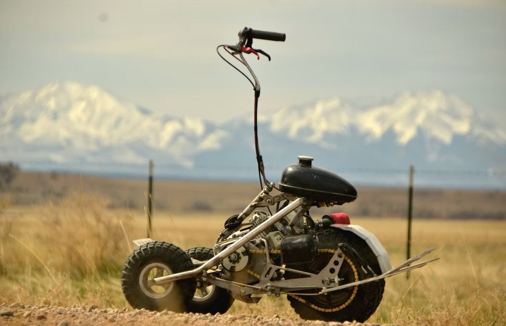
Developed by Eyal Aloni, the TLTBoard is a vehicle with side-stabilizing wheels. It combines design elements from a snowboard, dirt bike, and skateboard to create a vehicle that glides over roads, gravel, and even sand.
Each model is either electric or gas-powered, has a swappable battery or fuel tank, and features a surfing-like driving position. This allows people to get used to the vehicle quickly.
Despite their rugged design, TLTBoards are lightweight. The heaviest model, the Gorilla, weighs 80 lbs, while the lightest, the Cruiser, weighs just 40 lbs. That makes them portable enough to carry into an office or load into the back of a truck with ease.
Since the TLTBoard’s primary use is outdoors, all models are designed to be dust-resistant and waterproof. However, if you damage one, you can repair it yourself since the company hasn’t used any proprietary components.
Which TLTBoard Should You Buy?
There are currently four TLTBoard models, each tailored for different riders and terrains. Your choice depends on how and where you plan to ride.
1. TLT Cruiser
For people looking to enter the outdoor vehicle world, the TLT Cruiser is a solid starting point at just $1,350. The model is noticeably lighter and more commuter-friendly, but can also handle off-road situations.
Specs-wise, it’s powered by a 48V 15A electric hub motor, capable of reaching 25 mph. It also features a swappable battery, providing up to 20 miles of range.
2. TLT Grizzly
While electric motors offer instant torque and power, they are somewhat limited in their capabilities, since finding an electric charger in the middle of the woods can be difficult. That’s where the TLT Grizzly comes in. Powered by a 160cc 4-stroke gas engine, the Grizzly is perfect for hardcore off-road enthusiasts.
You can explore remote trails without battery anxiety, and it’s pretty fast, reaching speeds of up to 40 mph. On a full tank, you can expect about 30 miles of range.
3. TLT Gorilla (Upcoming)
For those looking to tackle challenging terrain, TLTBoard is developing a new model: the Gorilla. It’s going to be powered by a chain-driven 1000W motor and could hit speeds of up to 35 mph, which is incredibly fast.
The device will also come with a swappable battery that, depending on your speed, should provide up to 20 miles of range. Plus, the vehicle would weigh around 80 lbs, making it relatively easy to transport.
4. TLT Racer (Upcoming)
Designed to be more agile and responsive, the TLT Runner will serve as a middle ground between the outdoor-focused Grizzly and the introductory Cruiser, making it perfect for both city streets and harsh terrains.
It will feature a 72V or 48V 30-amps electric hub motor, allowing riders to handle sudden changes or potholes while maintaining a steady speed of up to 35 mph. Like the Gorilla, it will offer a 20-mile range on a single charge, and the battery will be swappable in just a few minutes. Additionally, it’ll weigh only 60 lbs.
Conclusion
Ultimately, TLTBoard aims to combine both urban and off-road capabilities into a single sports machine that checks every box and tackles any terrain without a hitch. It essentially becomes an extension of the body, going where the flow dictates, rather than requiring a significant learning curve. With a diverse current and upcoming lineup, there’s something for everyone, and the future of all-terrain electric (and gas-powered) vehicles looks especially promising.
Source link
#TLTBoard #Future #Outdoor #Mobility
![‘Alice in Borderland: Retry’ Makes Up For the Netflix Series Reheating ‘Squid Game’ Nachos
Not to pick at an irritated scab, but when the eighth and final season of Game of Thrones… happened… I, a fan of the series via the show, naively assumed all author George R.R. Martin had to do was pen a different bookend to the series to recover all the lost goodwill of the series. Little did I know that was a touchy subject among book-readers who’ve been tortured by the author’s perpetual procrastination for years. Condolences. While the same scenario isn’t fully analogous with what’s happened with Netflix’s live-action Alice in Borderland TV show and VIZ Media’s English manga release of the series’ extended epilogue, Alice in Borderland: Retry, the manga more than retroactively makes up for the huge disappointment I felt witnessing the show I loved go full Squid Game in the worst way possible in its final season. [embed]https://www.youtube.com/watch?v=49_44FFKZ1M[/embed] Alice in Borderland is a cutting series in which a man named Arisu gets trapped in a sci-fi death game where a group of sequestered survivors must compete in a litany of challenges in an abandoned city. Think Gantz meets Kaiji. Its rules are cruel, but never completely ass-pull, with players logically outfoxing each other to win games lest a laser from the sky punch them through the top of their heads.
The show was so good I didn’t realize it was based on a manga by Haro Aso (Zom 100: Bucketlist of the Dead) that was also adapted into an anime—a fact that speaks to its overall quality in a sea of lackluster live-action Netflix projects. And for two seasons it came and went, adapting that story prior to Squid Game mania and, subsequently, in the throes of its pop culture takeover. That is, until a third season was released last year, ripping Arisu and his lover Usagi from their peaceful lives post-death games and throwing them back into the fray like a kid with a magnifying glass looming over an ant hill.
[embed]https://www.youtube.com/watch?v=_8p6YkEPVco[/embed] I was rocking with the series for a bit despite the show clearly making stuff up as it went along until it committed the tacky, cardinal sin of copying what Squid Game’s third season did in its final moments, desperately sequel-baiting itself by asking the question no one was curious about in a stinger: What if it took place in America? May that answer never come because of the road it took to tarnish the show’s reputation. As far as I’m concerned, there was no third season. Alice in Borderland Retry is now available in print and digital! Read a free preview: https://t.co/OJcjm9wliH pic.twitter.com/8iqGzwjTIV — VIZ Media (@VIZMedia) July 21, 2026 So imagine my surprise to find that Viz Media’s recently released localization of Aso’s 2020 epilogue manga to the series, set 10 years after its conclusion, would retroactively act as a remedy to the Netflix series’ final season I wish I could wipe from my mind palace. The manga starts out almost exactly the same as the third season of the Netflix series (duh, the manga came out first), with Arisu going from a NEET to a psychologist and Usagi expecting their first child. That’s the last thing similar between the two.
Unlike the Netflix series’ contrived reasoning to get everyone back into the games, Arisu winds up in the games for a pretty simple reason. He and five other participants get hit by a billboard and wind up in the Borderlands. If you’ve watched the show or read the manga, this inciting incident is far from the cataclysmic events that send Arisu to the Borderlands the first time around, but what it lacks in spectacle, it more than makes up for in the challenge that awaits them. In contrast to the more-is-more inventiveness of the Netflix series’ games in its final season, Arisu and company only have to play one game, which is essentially musical chairs but for keeps. Despite the simplicity of the game, the stakes of the 300+ page epilogue far exceed those of the Netflix series, where its collective of players, composed of an insurance employee, a nursery school teacher, an emergency room nurse, a doctor, and an unemployed man, have to debate whose life matters more. [embed]https://www.youtube.com/watch?v=Dq2p_B5MD0c[/embed] It’s rare that manga get a chance to reach a conclusion without getting the axe, and just as rare for series on an indefinite hiatus to start back up regardless of whether a creator is healthy, willing, and able to spin more narrative yarn years after the fact. Which begs the question whether the juice is worth the squeeze to loop back to a series that’s already over. Evidently, I wasn’t the only one in doubt of what, if anything, could be gained from revisiting a series whose manga concluded pretty succinctly. Aso had his doubts too, which he lays bare near the midpoint of the manga, writing the following:
It’s been ten years since I started working on Alice in Borderland. Like Arisu, I didn’t want to ever revisit a horrifying world like Borderland, but I was given the opportunity to write a sequel and I just couldn’t pass it up. What does it mean to live? What do our lives mean? Now, at 40 years old, I want to retry answering these questions. While its game is a deceptively simple one, a fatal road of agony, betrayal, and second-guessing the inherent good in the human spirit left me in awe as I flipped through its pages and found that Aso still had it in him to concoct an intense, not-so-unwinnable death game, and that what he had to say serves as a footnote to a series that’s more than earned its place in the pantheon of death game narratives. Want more io9 news? Check out when to expect the latest Marvel, Star Wars, and Star Trek releases, what’s next for the DC Universe on film and TV, and everything you need to know about the future of Doctor Who. #Alice #Borderland #Retry #Netflix #Series #Reheating #Squid #Game #NachosAlice in Borderland,Manga,Netflix,Viz Media](https://i2.wp.com/gizmodo.com/app/uploads/2026/07/Alice-in-Borderland-1280x853.jpg?ssl=1 "‘Alice in Borderland: Retry’ Makes Up For the Netflix Series Reheating ‘Squid Game’ Nachos
Not to pick at an irritated scab, but when the eighth and final season of Game of Thrones… happened… I, a fan of the series via the show, naively assumed all author George R.R. Martin had to do was pen a different bookend to the series to recover all the lost goodwill of the series. Little did I know that was a touchy subject among book-readers who’ve been tortured by the author’s perpetual procrastination for years. Condolences. While the same scenario isn’t fully analogous with what’s happened with Netflix’s live-action Alice in Borderland TV show and VIZ Media’s English manga release of the series’ extended epilogue, Alice in Borderland: Retry, the manga more than retroactively makes up for the huge disappointment I felt witnessing the show I loved go full Squid Game in the worst way possible in its final season. [embed]https://www.youtube.com/watch?v=49_44FFKZ1M[/embed] Alice in Borderland is a cutting series in which a man named Arisu gets trapped in a sci-fi death game where a group of sequestered survivors must compete in a litany of challenges in an abandoned city. Think Gantz meets Kaiji. Its rules are cruel, but never completely ass-pull, with players logically outfoxing each other to win games lest a laser from the sky punch them through the top of their heads.
The show was so good I didn’t realize it was based on a manga by Haro Aso (Zom 100: Bucketlist of the Dead) that was also adapted into an anime—a fact that speaks to its overall quality in a sea of lackluster live-action Netflix projects. And for two seasons it came and went, adapting that story prior to Squid Game mania and, subsequently, in the throes of its pop culture takeover. That is, until a third season was released last year, ripping Arisu and his lover Usagi from their peaceful lives post-death games and throwing them back into the fray like a kid with a magnifying glass looming over an ant hill.
[embed]https://www.youtube.com/watch?v=_8p6YkEPVco[/embed] I was rocking with the series for a bit despite the show clearly making stuff up as it went along until it committed the tacky, cardinal sin of copying what Squid Game’s third season did in its final moments, desperately sequel-baiting itself by asking the question no one was curious about in a stinger: What if it took place in America? May that answer never come because of the road it took to tarnish the show’s reputation. As far as I’m concerned, there was no third season. Alice in Borderland Retry is now available in print and digital! Read a free preview: https://t.co/OJcjm9wliH pic.twitter.com/8iqGzwjTIV — VIZ Media (@VIZMedia) July 21, 2026 So imagine my surprise to find that Viz Media’s recently released localization of Aso’s 2020 epilogue manga to the series, set 10 years after its conclusion, would retroactively act as a remedy to the Netflix series’ final season I wish I could wipe from my mind palace. The manga starts out almost exactly the same as the third season of the Netflix series (duh, the manga came out first), with Arisu going from a NEET to a psychologist and Usagi expecting their first child. That’s the last thing similar between the two.
Unlike the Netflix series’ contrived reasoning to get everyone back into the games, Arisu winds up in the games for a pretty simple reason. He and five other participants get hit by a billboard and wind up in the Borderlands. If you’ve watched the show or read the manga, this inciting incident is far from the cataclysmic events that send Arisu to the Borderlands the first time around, but what it lacks in spectacle, it more than makes up for in the challenge that awaits them. In contrast to the more-is-more inventiveness of the Netflix series’ games in its final season, Arisu and company only have to play one game, which is essentially musical chairs but for keeps. Despite the simplicity of the game, the stakes of the 300+ page epilogue far exceed those of the Netflix series, where its collective of players, composed of an insurance employee, a nursery school teacher, an emergency room nurse, a doctor, and an unemployed man, have to debate whose life matters more. [embed]https://www.youtube.com/watch?v=Dq2p_B5MD0c[/embed] It’s rare that manga get a chance to reach a conclusion without getting the axe, and just as rare for series on an indefinite hiatus to start back up regardless of whether a creator is healthy, willing, and able to spin more narrative yarn years after the fact. Which begs the question whether the juice is worth the squeeze to loop back to a series that’s already over. Evidently, I wasn’t the only one in doubt of what, if anything, could be gained from revisiting a series whose manga concluded pretty succinctly. Aso had his doubts too, which he lays bare near the midpoint of the manga, writing the following:
It’s been ten years since I started working on Alice in Borderland. Like Arisu, I didn’t want to ever revisit a horrifying world like Borderland, but I was given the opportunity to write a sequel and I just couldn’t pass it up. What does it mean to live? What do our lives mean? Now, at 40 years old, I want to retry answering these questions. While its game is a deceptively simple one, a fatal road of agony, betrayal, and second-guessing the inherent good in the human spirit left me in awe as I flipped through its pages and found that Aso still had it in him to concoct an intense, not-so-unwinnable death game, and that what he had to say serves as a footnote to a series that’s more than earned its place in the pantheon of death game narratives. Want more io9 news? Check out when to expect the latest Marvel, Star Wars, and Star Trek releases, what’s next for the DC Universe on film and TV, and everything you need to know about the future of Doctor Who. #Alice #Borderland #Retry #Netflix #Series #Reheating #Squid #Game #NachosAlice in Borderland,Manga,Netflix,Viz Media")
![‘Alice in Borderland: Retry’ Makes Up For the Netflix Series Reheating ‘Squid Game’ Nachos
Not to pick at an irritated scab, but when the eighth and final season of Game of Thrones… happened… I, a fan of the series via the show, naively assumed all author George R.R. Martin had to do was pen a different bookend to the series to recover all the lost goodwill of the series. Little did I know that was a touchy subject among book-readers who’ve been tortured by the author’s perpetual procrastination for years. Condolences. While the same scenario isn’t fully analogous with what’s happened with Netflix’s live-action Alice in Borderland TV show and VIZ Media’s English manga release of the series’ extended epilogue, Alice in Borderland: Retry, the manga more than retroactively makes up for the huge disappointment I felt witnessing the show I loved go full Squid Game in the worst way possible in its final season. [embed]https://www.youtube.com/watch?v=49_44FFKZ1M[/embed] Alice in Borderland is a cutting series in which a man named Arisu gets trapped in a sci-fi death game where a group of sequestered survivors must compete in a litany of challenges in an abandoned city. Think Gantz meets Kaiji. Its rules are cruel, but never completely ass-pull, with players logically outfoxing each other to win games lest a laser from the sky punch them through the top of their heads.
The show was so good I didn’t realize it was based on a manga by Haro Aso (Zom 100: Bucketlist of the Dead) that was also adapted into an anime—a fact that speaks to its overall quality in a sea of lackluster live-action Netflix projects. And for two seasons it came and went, adapting that story prior to Squid Game mania and, subsequently, in the throes of its pop culture takeover. That is, until a third season was released last year, ripping Arisu and his lover Usagi from their peaceful lives post-death games and throwing them back into the fray like a kid with a magnifying glass looming over an ant hill.
[embed]https://www.youtube.com/watch?v=_8p6YkEPVco[/embed] I was rocking with the series for a bit despite the show clearly making stuff up as it went along until it committed the tacky, cardinal sin of copying what Squid Game’s third season did in its final moments, desperately sequel-baiting itself by asking the question no one was curious about in a stinger: What if it took place in America? May that answer never come because of the road it took to tarnish the show’s reputation. As far as I’m concerned, there was no third season. Alice in Borderland Retry is now available in print and digital! Read a free preview: https://t.co/OJcjm9wliH pic.twitter.com/8iqGzwjTIV — VIZ Media (@VIZMedia) July 21, 2026 So imagine my surprise to find that Viz Media’s recently released localization of Aso’s 2020 epilogue manga to the series, set 10 years after its conclusion, would retroactively act as a remedy to the Netflix series’ final season I wish I could wipe from my mind palace. The manga starts out almost exactly the same as the third season of the Netflix series (duh, the manga came out first), with Arisu going from a NEET to a psychologist and Usagi expecting their first child. That’s the last thing similar between the two.
Unlike the Netflix series’ contrived reasoning to get everyone back into the games, Arisu winds up in the games for a pretty simple reason. He and five other participants get hit by a billboard and wind up in the Borderlands. If you’ve watched the show or read the manga, this inciting incident is far from the cataclysmic events that send Arisu to the Borderlands the first time around, but what it lacks in spectacle, it more than makes up for in the challenge that awaits them. In contrast to the more-is-more inventiveness of the Netflix series’ games in its final season, Arisu and company only have to play one game, which is essentially musical chairs but for keeps. Despite the simplicity of the game, the stakes of the 300+ page epilogue far exceed those of the Netflix series, where its collective of players, composed of an insurance employee, a nursery school teacher, an emergency room nurse, a doctor, and an unemployed man, have to debate whose life matters more. [embed]https://www.youtube.com/watch?v=Dq2p_B5MD0c[/embed] It’s rare that manga get a chance to reach a conclusion without getting the axe, and just as rare for series on an indefinite hiatus to start back up regardless of whether a creator is healthy, willing, and able to spin more narrative yarn years after the fact. Which begs the question whether the juice is worth the squeeze to loop back to a series that’s already over. Evidently, I wasn’t the only one in doubt of what, if anything, could be gained from revisiting a series whose manga concluded pretty succinctly. Aso had his doubts too, which he lays bare near the midpoint of the manga, writing the following:
It’s been ten years since I started working on Alice in Borderland. Like Arisu, I didn’t want to ever revisit a horrifying world like Borderland, but I was given the opportunity to write a sequel and I just couldn’t pass it up. What does it mean to live? What do our lives mean? Now, at 40 years old, I want to retry answering these questions. While its game is a deceptively simple one, a fatal road of agony, betrayal, and second-guessing the inherent good in the human spirit left me in awe as I flipped through its pages and found that Aso still had it in him to concoct an intense, not-so-unwinnable death game, and that what he had to say serves as a footnote to a series that’s more than earned its place in the pantheon of death game narratives. Want more io9 news? Check out when to expect the latest Marvel, Star Wars, and Star Trek releases, what’s next for the DC Universe on film and TV, and everything you need to know about the future of Doctor Who. #Alice #Borderland #Retry #Netflix #Series #Reheating #Squid #Game #NachosAlice in Borderland,Manga,Netflix,Viz Media](https://gizmodo.com/app/uploads/2026/07/Alice-in-Borderland-1280x853.jpg "‘Alice in Borderland: Retry’ Makes Up For the Netflix Series Reheating ‘Squid Game’ Nachos
Not to pick at an irritated scab, but when the eighth and final season of Game of Thrones… happened… I, a fan of the series via the show, naively assumed all author George R.R. Martin had to do was pen a different bookend to the series to recover all the lost goodwill of the series. Little did I know that was a touchy subject among book-readers who’ve been tortured by the author’s perpetual procrastination for years. Condolences. While the same scenario isn’t fully analogous with what’s happened with Netflix’s live-action Alice in Borderland TV show and VIZ Media’s English manga release of the series’ extended epilogue, Alice in Borderland: Retry, the manga more than retroactively makes up for the huge disappointment I felt witnessing the show I loved go full Squid Game in the worst way possible in its final season. [embed]https://www.youtube.com/watch?v=49_44FFKZ1M[/embed] Alice in Borderland is a cutting series in which a man named Arisu gets trapped in a sci-fi death game where a group of sequestered survivors must compete in a litany of challenges in an abandoned city. Think Gantz meets Kaiji. Its rules are cruel, but never completely ass-pull, with players logically outfoxing each other to win games lest a laser from the sky punch them through the top of their heads.
The show was so good I didn’t realize it was based on a manga by Haro Aso (Zom 100: Bucketlist of the Dead) that was also adapted into an anime—a fact that speaks to its overall quality in a sea of lackluster live-action Netflix projects. And for two seasons it came and went, adapting that story prior to Squid Game mania and, subsequently, in the throes of its pop culture takeover. That is, until a third season was released last year, ripping Arisu and his lover Usagi from their peaceful lives post-death games and throwing them back into the fray like a kid with a magnifying glass looming over an ant hill.
[embed]https://www.youtube.com/watch?v=_8p6YkEPVco[/embed] I was rocking with the series for a bit despite the show clearly making stuff up as it went along until it committed the tacky, cardinal sin of copying what Squid Game’s third season did in its final moments, desperately sequel-baiting itself by asking the question no one was curious about in a stinger: What if it took place in America? May that answer never come because of the road it took to tarnish the show’s reputation. As far as I’m concerned, there was no third season. Alice in Borderland Retry is now available in print and digital! Read a free preview: https://t.co/OJcjm9wliH pic.twitter.com/8iqGzwjTIV — VIZ Media (@VIZMedia) July 21, 2026 So imagine my surprise to find that Viz Media’s recently released localization of Aso’s 2020 epilogue manga to the series, set 10 years after its conclusion, would retroactively act as a remedy to the Netflix series’ final season I wish I could wipe from my mind palace. The manga starts out almost exactly the same as the third season of the Netflix series (duh, the manga came out first), with Arisu going from a NEET to a psychologist and Usagi expecting their first child. That’s the last thing similar between the two.
Unlike the Netflix series’ contrived reasoning to get everyone back into the games, Arisu winds up in the games for a pretty simple reason. He and five other participants get hit by a billboard and wind up in the Borderlands. If you’ve watched the show or read the manga, this inciting incident is far from the cataclysmic events that send Arisu to the Borderlands the first time around, but what it lacks in spectacle, it more than makes up for in the challenge that awaits them. In contrast to the more-is-more inventiveness of the Netflix series’ games in its final season, Arisu and company only have to play one game, which is essentially musical chairs but for keeps. Despite the simplicity of the game, the stakes of the 300+ page epilogue far exceed those of the Netflix series, where its collective of players, composed of an insurance employee, a nursery school teacher, an emergency room nurse, a doctor, and an unemployed man, have to debate whose life matters more. [embed]https://www.youtube.com/watch?v=Dq2p_B5MD0c[/embed] It’s rare that manga get a chance to reach a conclusion without getting the axe, and just as rare for series on an indefinite hiatus to start back up regardless of whether a creator is healthy, willing, and able to spin more narrative yarn years after the fact. Which begs the question whether the juice is worth the squeeze to loop back to a series that’s already over. Evidently, I wasn’t the only one in doubt of what, if anything, could be gained from revisiting a series whose manga concluded pretty succinctly. Aso had his doubts too, which he lays bare near the midpoint of the manga, writing the following:
It’s been ten years since I started working on Alice in Borderland. Like Arisu, I didn’t want to ever revisit a horrifying world like Borderland, but I was given the opportunity to write a sequel and I just couldn’t pass it up. What does it mean to live? What do our lives mean? Now, at 40 years old, I want to retry answering these questions. While its game is a deceptively simple one, a fatal road of agony, betrayal, and second-guessing the inherent good in the human spirit left me in awe as I flipped through its pages and found that Aso still had it in him to concoct an intense, not-so-unwinnable death game, and that what he had to say serves as a footnote to a series that’s more than earned its place in the pantheon of death game narratives. Want more io9 news? Check out when to expect the latest Marvel, Star Wars, and Star Trek releases, what’s next for the DC Universe on film and TV, and everything you need to know about the future of Doctor Who. #Alice #Borderland #Retry #Netflix #Series #Reheating #Squid #Game #NachosAlice in Borderland,Manga,Netflix,Viz Media")
The new Chinese models have a few things in common: Third-party benchmarks show that they perform nearly as well as the best Western models; they are optimized for agentic coding tasks (the hottest thing in AI this year); and they are or will soon be released with open weights, making them accessible and transparent.But perhaps the biggest parallel between the current moment and January 2025—when the world was shocked by DeepSeek’s R1 model—is that it reaffirms how American and Chinese AI labs are taking diverging paths when it comes to being open or closed.When it first burst onto the scene, DeepSeek challenged the premise that only closed-source models built with billions of dollars of investment in compute infrastructure and training could achieve frontier performance. But since then, Western AI labs have continued developing AI the same way, and now American frontier models feel more roped-off than they were a year ago.Anthropic said for months that its latest Mythos model was so dangerously good at hacking that only approved collaborators could use it. When it was finally released more widely, the White House responded by issuing broad export controls, which forced Anthropic to take Mythos and its less capable sister model, Fable 5, offline temporarily. OpenAI similarly delayed the release of GPT 5.6 after it received a request from the White House.In China, meanwhile, the situation looks very different. Chinese startups and tech giants have doubled down on open source: Anyone with a good enough computer environment can now download an open-weight model, run it locally, add customizations, and overall enjoy a much greater degree of freedom than OpenAI and Anthropic would ever allow. In many ways, the open versus closed debate is more entangled with the US versus China debate than ever before.There are a lot of reasons why Chinese labs have chosen a business strategy built atop open-source models. Being the newer, smaller fish in the AI field, making their models free and open can help Chinese firms attract more users, collaborators, and media spotlight. It also puts them in a separate lane of competition from the one that OpenAI, Anthropic, Google, SpaceX, and other deep-pocketed giants are in.Earlier this year, rumors spread that Alibaba might be considering joining the closed-source race after it rearranged its corporate AI model development teams. But the tech giant announced on Monday that it would again release the latest version of Qwen—its line of open-source models beloved by the global tech community—with open weights, signaling to customers and the public it is not pivoting away yet.#Chinas #Open #Models #Challenging #Silicon #Valleys #Playbookchina,open source,alibaba,generative ai,national security,artificial intelligence")

Post Comment