
Before the end of 2025, Disney surprised everyone (derogatory) by entering into a $1 billion deal with OpenAI. With it, over 200 Disney characters have been licensed for the Sora video platform and image generator ChatGPT. From the general public and Hollywood alike, reactions weren’t exactly thrilled, but SAG-AFTRA is keeping an open mind. Sort of.
Talking to Deadline at CES, union presidents Sean Astin and Duncan Crabtree-Ireland were asked what the deal could mean for the acting industry. In 2023 and 2024, SAG-AFTRA went on strike to secure better protections against synthetic performers and actors being made to sign their voice rights away. Crabtree-Ireland admitted he doesn’t know the full details of the agreement made between the two companies but revealed they contacted SAG-AFTRA before the public reveal.
In the call announcing the deal, “top execs” from Disney and OpenAI said the deal has “certain assurances,” such as “explicitly excluding any licensing of any performer images or voices,” explained Crabtree-Ireland. “One concern I have, and I expect Sean shares, is precisely why Disney would want to do it. Making a deal like that before the IP litigation, copyright litigation is resolved, could be smart.”
While Disney can’t be stopped from partnering with OpenAI, SAG-AFTRA knows it’s made progress where it can. Crabtree-Ireland noted the union’s contract from 2023 requires companies to proactively disclose if they’ve created and used a synthetic performance, of which there’ve been “zero notices” about so far. But they’re not stopping there: every future negotiation SAG-AFTRA takes part in will involve “looking at how AI is rolling out and developing.” Machine learning technology has greatly evolved in recent years, and the hope is to “continue creating separation between AI, as an algorithmic tool, and humanity.”
Want more io9 news? Check out when to expect the latest Marvel, Star Wars, and Star Trek releases, what’s next for the DC Universe on film and TV, and everything you need to know about the future of Doctor Who.
Source link
#SAGAFTRA #Keeping #Eye #DisneyOpenAI #Deal


![IBM Crosses One of Computing’s Biggest Barriers With World’s First Sub-1 Nanometer Chip
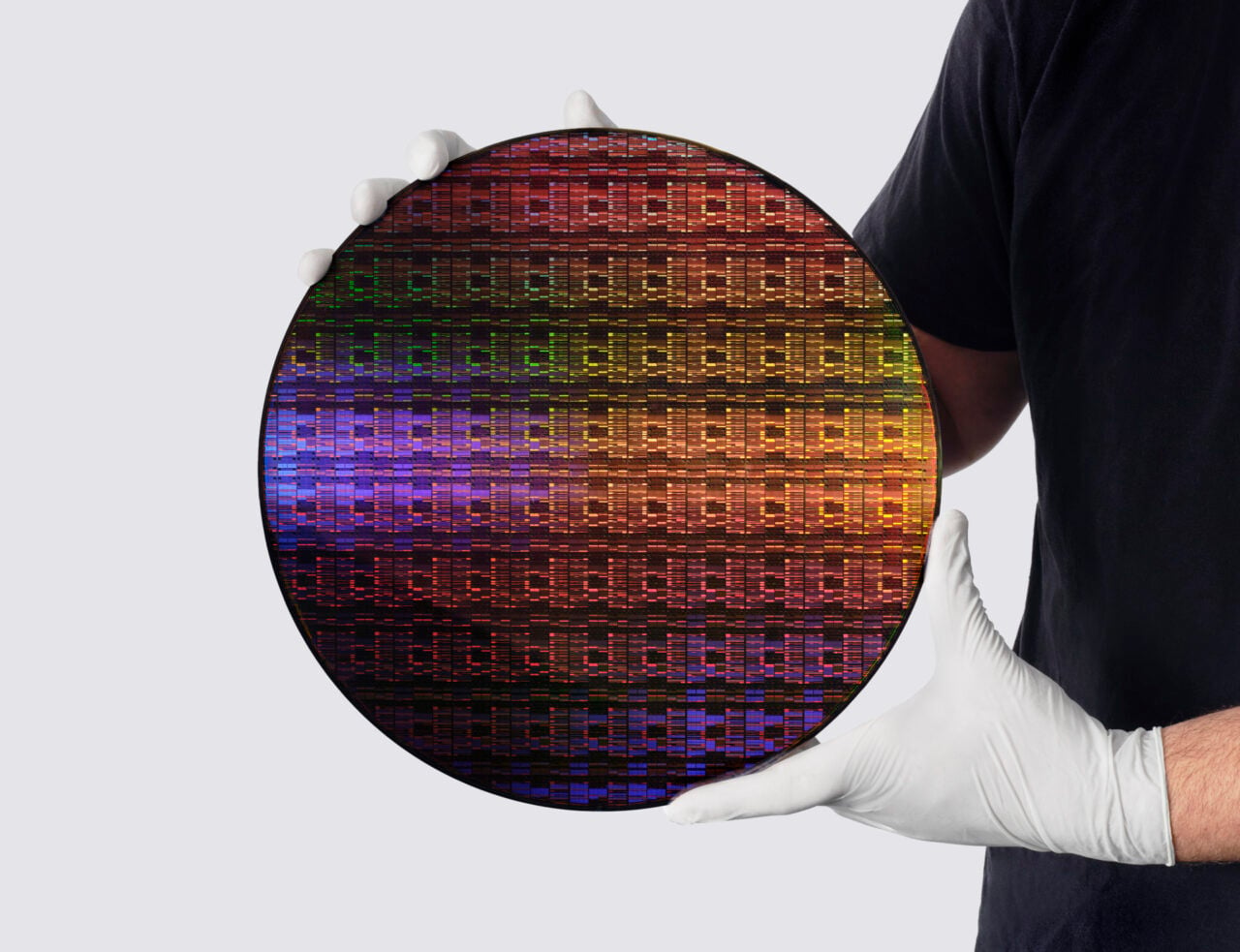
In a major breakthrough, IBM revealed the world’s first semiconductor chip technology built on a sub-1 nanometer chipmaking process. For comparison, the process uses transistor features smaller than the width of a DNA strand, which measures about 2.5 nanometers across. The chip itself is about the size of a fingernail but holds almost 100 billion transistors, and the company expects it could enter markets as early as the next five years. In a statement released today, IBM said the new chip features nearly twice the density of its 2-nanometer chip, released in 2021. According to an accompanying technical report, the chip also demonstrated up to 70% greater energy efficiency than its predecessor. In designing the chip, researchers developed an “entirely new transistor architecture” called nanostack, which “vertically stacks and staggers transistors” to enable IBM’s 0.7-nanometer chip technology, IBM explained. A section of the chip seen with a transmission electron microscope. Credit: IBM “With our new nanostack architecture, we’re not just making smaller transistors,” Jay Gambetta, director of IBM Research, said in the statement. “We’re reinventing how chips are built to deliver dramatically more power and energy efficiency.”
Smaller and smaller Semiconductor chips enable things like computers, home appliances, communications, and transportation devices. In 1965, Intel co-founder Gordon Moore surmised that transistor capacities evolved at a predictable and consistent rate. Specifically, all things considered, the number of transistors on a semiconductor chip would double about every two years. For a while, the so-called Moore’s Law held rather well—until, that is, things hit a literal wall.
“Moore’s Law was never meant to last forever,” according to a blog post by the Massachusetts Institute of Technology’s (MIT) Computer Science and Artificial Intelligence Lab. “Transistors can only get so small and, eventually, the more permanent laws of physics get in the way.” That is, as companies try to cram more transistors into smaller chips, new advances in transistor technology take longer than two years, so Moore’s Law has been over since at least 2016, Charles Leiserson, a computer scientist at MIT, said in the blog. Accordingly, the issue now is to consider how improvements in chip performance fit into a longer-term picture, Willy Shih, an economist at Harvard Business School, said in an explainer.
Reaching atomic levels In that sense, IBM’s latest chip represents an inventive approach for bypassing the limits of physical scaling. Specifically, two wafers with nanosheet-style transistors are glued together like a sandwich to vertically stack two layers of transistors, and related technical assessments suggested that the wafer stacking was flexible and scalable enough to support real computation, Huiming Bu, vice president of IBM’s silicon technology research team, said in a press briefing on the chip. Researcher holding IBM’s sub-1 nm node wafer. Credit: IBM That said, this chip isn’t quite ready for manufacturing just yet. The company’s goal is to enter production in the next five years, but there’s still work to be done. For instance, Bu pointed out that the team was still working on pathways to prevent thermal noise or integration into existing systems in the high-performance computing community. “From my perspective, I hope to see it be as successful as the 2-nanometer [chip] and become the industry platform,” Gambetta said during the briefing. “And as we see with AI and classical computing in general, we are only seeing more and more consumption.” #IBM #Crosses #Computings #Biggest #Barriers #Worlds #Sub1 #Nanometer #ChipIBM,Semiconductors,transistors](https://gizmodo.com/app/uploads/2026/06/nanostacking-ibm-sub-nm-chip-1280x720.jpg "IBM Crosses One of Computing’s Biggest Barriers With World’s First Sub-1 Nanometer Chip
In a major breakthrough, IBM revealed the world’s first semiconductor chip technology built on a sub-1 nanometer chipmaking process. For comparison, the process uses transistor features smaller than the width of a DNA strand, which measures about 2.5 nanometers across. The chip itself is about the size of a fingernail but holds almost 100 billion transistors, and the company expects it could enter markets as early as the next five years. In a statement released today, IBM said the new chip features nearly twice the density of its 2-nanometer chip, released in 2021. According to an accompanying technical report, the chip also demonstrated up to 70% greater energy efficiency than its predecessor. In designing the chip, researchers developed an “entirely new transistor architecture” called nanostack, which “vertically stacks and staggers transistors” to enable IBM’s 0.7-nanometer chip technology, IBM explained. A section of the chip seen with a transmission electron microscope. Credit: IBM “With our new nanostack architecture, we’re not just making smaller transistors,” Jay Gambetta, director of IBM Research, said in the statement. “We’re reinventing how chips are built to deliver dramatically more power and energy efficiency.”
Smaller and smaller Semiconductor chips enable things like computers, home appliances, communications, and transportation devices. In 1965, Intel co-founder Gordon Moore surmised that transistor capacities evolved at a predictable and consistent rate. Specifically, all things considered, the number of transistors on a semiconductor chip would double about every two years. For a while, the so-called Moore’s Law held rather well—until, that is, things hit a literal wall.
“Moore’s Law was never meant to last forever,” according to a blog post by the Massachusetts Institute of Technology’s (MIT) Computer Science and Artificial Intelligence Lab. “Transistors can only get so small and, eventually, the more permanent laws of physics get in the way.” That is, as companies try to cram more transistors into smaller chips, new advances in transistor technology take longer than two years, so Moore’s Law has been over since at least 2016, Charles Leiserson, a computer scientist at MIT, said in the blog. Accordingly, the issue now is to consider how improvements in chip performance fit into a longer-term picture, Willy Shih, an economist at Harvard Business School, said in an explainer.
Reaching atomic levels In that sense, IBM’s latest chip represents an inventive approach for bypassing the limits of physical scaling. Specifically, two wafers with nanosheet-style transistors are glued together like a sandwich to vertically stack two layers of transistors, and related technical assessments suggested that the wafer stacking was flexible and scalable enough to support real computation, Huiming Bu, vice president of IBM’s silicon technology research team, said in a press briefing on the chip. Researcher holding IBM’s sub-1 nm node wafer. Credit: IBM That said, this chip isn’t quite ready for manufacturing just yet. The company’s goal is to enter production in the next five years, but there’s still work to be done. For instance, Bu pointed out that the team was still working on pathways to prevent thermal noise or integration into existing systems in the high-performance computing community. “From my perspective, I hope to see it be as successful as the 2-nanometer [chip] and become the industry platform,” Gambetta said during the briefing. “And as we see with AI and classical computing in general, we are only seeing more and more consumption.” #IBM #Crosses #Computings #Biggest #Barriers #Worlds #Sub1 #Nanometer #ChipIBM,Semiconductors,transistors")
![IBM Crosses One of Computing’s Biggest Barriers With World’s First Sub-1 Nanometer Chip
In a major breakthrough, IBM revealed the world’s first semiconductor chip technology built on a sub-1 nanometer chipmaking process. For comparison, the process uses transistor features smaller than the width of a DNA strand, which measures about 2.5 nanometers across. The chip itself is about the size of a fingernail but holds almost 100 billion transistors, and the company expects it could enter markets as early as the next five years. In a statement released today, IBM said the new chip features nearly twice the density of its 2-nanometer chip, released in 2021. According to an accompanying technical report, the chip also demonstrated up to 70% greater energy efficiency than its predecessor. In designing the chip, researchers developed an “entirely new transistor architecture” called nanostack, which “vertically stacks and staggers transistors” to enable IBM’s 0.7-nanometer chip technology, IBM explained. A section of the chip seen with a transmission electron microscope. Credit: IBM “With our new nanostack architecture, we’re not just making smaller transistors,” Jay Gambetta, director of IBM Research, said in the statement. “We’re reinventing how chips are built to deliver dramatically more power and energy efficiency.”
Smaller and smaller Semiconductor chips enable things like computers, home appliances, communications, and transportation devices. In 1965, Intel co-founder Gordon Moore surmised that transistor capacities evolved at a predictable and consistent rate. Specifically, all things considered, the number of transistors on a semiconductor chip would double about every two years. For a while, the so-called Moore’s Law held rather well—until, that is, things hit a literal wall.
“Moore’s Law was never meant to last forever,” according to a blog post by the Massachusetts Institute of Technology’s (MIT) Computer Science and Artificial Intelligence Lab. “Transistors can only get so small and, eventually, the more permanent laws of physics get in the way.” That is, as companies try to cram more transistors into smaller chips, new advances in transistor technology take longer than two years, so Moore’s Law has been over since at least 2016, Charles Leiserson, a computer scientist at MIT, said in the blog. Accordingly, the issue now is to consider how improvements in chip performance fit into a longer-term picture, Willy Shih, an economist at Harvard Business School, said in an explainer.
Reaching atomic levels In that sense, IBM’s latest chip represents an inventive approach for bypassing the limits of physical scaling. Specifically, two wafers with nanosheet-style transistors are glued together like a sandwich to vertically stack two layers of transistors, and related technical assessments suggested that the wafer stacking was flexible and scalable enough to support real computation, Huiming Bu, vice president of IBM’s silicon technology research team, said in a press briefing on the chip. Researcher holding IBM’s sub-1 nm node wafer. Credit: IBM That said, this chip isn’t quite ready for manufacturing just yet. The company’s goal is to enter production in the next five years, but there’s still work to be done. For instance, Bu pointed out that the team was still working on pathways to prevent thermal noise or integration into existing systems in the high-performance computing community. “From my perspective, I hope to see it be as successful as the 2-nanometer [chip] and become the industry platform,” Gambetta said during the briefing. “And as we see with AI and classical computing in general, we are only seeing more and more consumption.” #IBM #Crosses #Computings #Biggest #Barriers #Worlds #Sub1 #Nanometer #ChipIBM,Semiconductors,transistors](https://i1.wp.com/gizmodo.com/app/uploads/2026/06/nanostacking-ibm-sub-nm-chip-1280x720.jpg?ssl=1 "IBM Crosses One of Computing’s Biggest Barriers With World’s First Sub-1 Nanometer Chip
In a major breakthrough, IBM revealed the world’s first semiconductor chip technology built on a sub-1 nanometer chipmaking process. For comparison, the process uses transistor features smaller than the width of a DNA strand, which measures about 2.5 nanometers across. The chip itself is about the size of a fingernail but holds almost 100 billion transistors, and the company expects it could enter markets as early as the next five years. In a statement released today, IBM said the new chip features nearly twice the density of its 2-nanometer chip, released in 2021. According to an accompanying technical report, the chip also demonstrated up to 70% greater energy efficiency than its predecessor. In designing the chip, researchers developed an “entirely new transistor architecture” called nanostack, which “vertically stacks and staggers transistors” to enable IBM’s 0.7-nanometer chip technology, IBM explained. A section of the chip seen with a transmission electron microscope. Credit: IBM “With our new nanostack architecture, we’re not just making smaller transistors,” Jay Gambetta, director of IBM Research, said in the statement. “We’re reinventing how chips are built to deliver dramatically more power and energy efficiency.”
Smaller and smaller Semiconductor chips enable things like computers, home appliances, communications, and transportation devices. In 1965, Intel co-founder Gordon Moore surmised that transistor capacities evolved at a predictable and consistent rate. Specifically, all things considered, the number of transistors on a semiconductor chip would double about every two years. For a while, the so-called Moore’s Law held rather well—until, that is, things hit a literal wall.
“Moore’s Law was never meant to last forever,” according to a blog post by the Massachusetts Institute of Technology’s (MIT) Computer Science and Artificial Intelligence Lab. “Transistors can only get so small and, eventually, the more permanent laws of physics get in the way.” That is, as companies try to cram more transistors into smaller chips, new advances in transistor technology take longer than two years, so Moore’s Law has been over since at least 2016, Charles Leiserson, a computer scientist at MIT, said in the blog. Accordingly, the issue now is to consider how improvements in chip performance fit into a longer-term picture, Willy Shih, an economist at Harvard Business School, said in an explainer.
Reaching atomic levels In that sense, IBM’s latest chip represents an inventive approach for bypassing the limits of physical scaling. Specifically, two wafers with nanosheet-style transistors are glued together like a sandwich to vertically stack two layers of transistors, and related technical assessments suggested that the wafer stacking was flexible and scalable enough to support real computation, Huiming Bu, vice president of IBM’s silicon technology research team, said in a press briefing on the chip. Researcher holding IBM’s sub-1 nm node wafer. Credit: IBM That said, this chip isn’t quite ready for manufacturing just yet. The company’s goal is to enter production in the next five years, but there’s still work to be done. For instance, Bu pointed out that the team was still working on pathways to prevent thermal noise or integration into existing systems in the high-performance computing community. “From my perspective, I hope to see it be as successful as the 2-nanometer [chip] and become the industry platform,” Gambetta said during the briefing. “And as we see with AI and classical computing in general, we are only seeing more and more consumption.” #IBM #Crosses #Computings #Biggest #Barriers #Worlds #Sub1 #Nanometer #ChipIBM,Semiconductors,transistors")


-SOURCE-Scott-Gilbertson.jpg)
-SOURCE-Scott-Gilbertson.jpg)
-SOURCE-Scott-Gilbertson.jpg)
 is my favorite 360 camera. The dual 14-mm (35-mm equivalent) lenses of the Max 2 each record up to a 1/2.3-inch chip, yielding what GoPro calls “True 8K” (10-bit) video. The larger sensors of the Max 2 provide sharper, clearer footage than other 360 cameras, and you can record 10-bit color in log for greater flexibility in post-production color grading—a capability you’d be hard-pressed to find in other 360 cameras. Even if editing log footage is too much work (I hear you), GoPro’s natural-looking color rendition in the default color profile is still the best I’ve tested.As with most GoPros, the Max 2 has three mounting options: folding fingers, a tripod hole, and a magnetic system. This means you can mount the Max 2 just about anywhere. It also has the simplest lens-cover replacement process. To do it, just twist off the lenses with your fingers and pop on the new ones. You’ll get all the usual GoPro video modes, including HyperSmooth video stabilization, horizon leveling, TimeWarp, and more.The one flaw in the Max 2 is its lackluster audio quality. The best way to avoid that issue is to pair the camera with a Bluetooth mic. Also note that if low-light video is on your list of must-haves in an action camera, the Insta360 X5 (below) is probably a better bet. For everyone else, though, this is the 360 camera to get—especially at this discounted price.The Best Action Camera for VloggingPhotograph: Scott GilbertsonPhotograph: Scott GilbertsonPhotograph: Scott GilbertsonThe Insta360 Ace Pro 2 (8/10 WIRED Recommends) combines a great Leica lens with an 8K-capable sensor and a handy flip-up rear screen, which is why it’s my favorite action camera for vlogging. The 8K video is not that great for action footage, but the camera is nice for slower shots, which you can crop and still export to 4K. The standout feature, though, is the rear screen. Other action cameras offer a small front screen to compose selfies, but the Ace Pro 2’s entire huge rear screen is there to help you frame yourself. The rear screen also simplifies shooting from the hip and nailing other unusual angles, especially when paired with the Xplorer Grip Pro ( off).#GoPro #Deals #Good #Youll #Jump #Cliffamazon prime day,cameras,gopro,shopping,deals,buying guides,amazon prime day deals")
Post Comment