
Today’s Wordle answer should be easy to solve if you keep up with the latest trends.
If you just want to be told today’s word, you can jump to the bottom of this article for today’s Wordle solution revealed. But if you’d rather solve it yourself, keep reading for some clues, tips, and strategies to assist you.
SEE ALSO:
Mahjong, Sudoku, free crossword, and more: Play games on Mashable
SEE ALSO:
NYT Connections hints today: Clues, answers for March 7, 2026
Where did Wordle come from?
Originally created by engineer Josh Wardle as a gift for his partner, Wordle rapidly spread to become an international phenomenon, with thousands of people around the globe playing every day. Alternate Wordle versions created by fans also sprang up, including battle royale Squabble, music identification game Heardle, and variations like Dordle and Quordle that make you guess multiple words at once.
Wordle eventually became so popular that it was purchased by the New York Times, and TikTok creators even livestream themselves playing.
What’s the best Wordle starting word?
The best Wordle starting word is the one that speaks to you. But if you prefer to be strategic in your approach, we have a few ideas to help you pick a word that might help you find the solution faster. One tip is to select a word that includes at least two different vowels, plus some common consonants like S, T, R, or N.
What happened to the Wordle archive?
The entire archive of past Wordle puzzles was originally available for anyone to enjoy whenever they felt like it, but it was later taken down, with the website’s creator stating it was done at the request of the New York Times. However, the New York Times then rolled out its own Wordle Archive, available only to NYT Games subscribers.
Is Wordle getting harder?
It might feel like Wordle is getting harder, but it actually isn’t any more difficult than when it first began. You can turn on Wordle‘s Hard Mode if you’re after more of a challenge, though.
SEE ALSO:
NYT Pips hints, answers for March 7, 2026
Here’s a subtle hint for today’s Wordle answer:
An iconic fashion publication.
Mashable Top Stories
Does today’s Wordle answer have a double letter?
There are no recurring letters.
Today’s Wordle is a 5-letter word that starts with…
Today’s Wordle starts with the letter V.
SEE ALSO:
Wordle-obsessed? These are the best word games to play IRL.
The Wordle answer today is…
Get your last guesses in now, because it’s your final chance to solve today’s Wordle before we reveal the solution.
Drumroll please!
The solution to today’s Wordle is…
VOGUE
Don’t feel down if you didn’t manage to guess it this time. There will be a new Wordle for you to stretch your brain with tomorrow, and we’ll be back again to guide you with more helpful hints. Are you also playing NYT Strands? See hints and answers for today’s Strands.
Reporting by Chance Townsend, Caitlin Welsh, Sam Haysom, Amanda Yeo, Shannon Connellan, Cecily Mauran, Mike Pearl, and Adam Rosenberg contributed to this article.
If you’re looking for more puzzles, Mashable’s got games now! Check out our games hub for Mahjong, Sudoku, free crossword, and more.
Not the day you’re after? Here’s the solution to yesterday’s Wordle.
Source link
#Wordle #today #answer #hints #March


![IBM Crosses One of Computing’s Biggest Barriers With World’s First Sub-1 Nanometer Chip
In a major breakthrough, IBM revealed the world’s first semiconductor chip technology built on a sub-1 nanometer chipmaking process. For comparison, the process uses transistor features smaller than the width of a DNA strand, which measures about 2.5 nanometers across. The chip itself is about the size of a fingernail but holds almost 100 billion transistors, and the company expects it could enter markets as early as the next five years. In a statement released today, IBM said the new chip features nearly twice the density of its 2-nanometer chip, released in 2021. According to an accompanying technical report, the chip also demonstrated up to 70% greater energy efficiency than its predecessor. In designing the chip, researchers developed an “entirely new transistor architecture” called nanostack, which “vertically stacks and staggers transistors” to enable IBM’s 0.7-nanometer chip technology, IBM explained. A section of the chip seen with a transmission electron microscope. Credit: IBM “With our new nanostack architecture, we’re not just making smaller transistors,” Jay Gambetta, director of IBM Research, said in the statement. “We’re reinventing how chips are built to deliver dramatically more power and energy efficiency.”
Smaller and smaller Semiconductor chips enable things like computers, home appliances, communications, and transportation devices. In 1965, Intel co-founder Gordon Moore surmised that transistor capacities evolved at a predictable and consistent rate. Specifically, all things considered, the number of transistors on a semiconductor chip would double about every two years. For a while, the so-called Moore’s Law held rather well—until, that is, things hit a literal wall.
“Moore’s Law was never meant to last forever,” according to a blog post by the Massachusetts Institute of Technology’s (MIT) Computer Science and Artificial Intelligence Lab. “Transistors can only get so small and, eventually, the more permanent laws of physics get in the way.” That is, as companies try to cram more transistors into smaller chips, new advances in transistor technology take longer than two years, so Moore’s Law has been over since at least 2016, Charles Leiserson, a computer scientist at MIT, said in the blog. Accordingly, the issue now is to consider how improvements in chip performance fit into a longer-term picture, Willy Shih, an economist at Harvard Business School, said in an explainer.
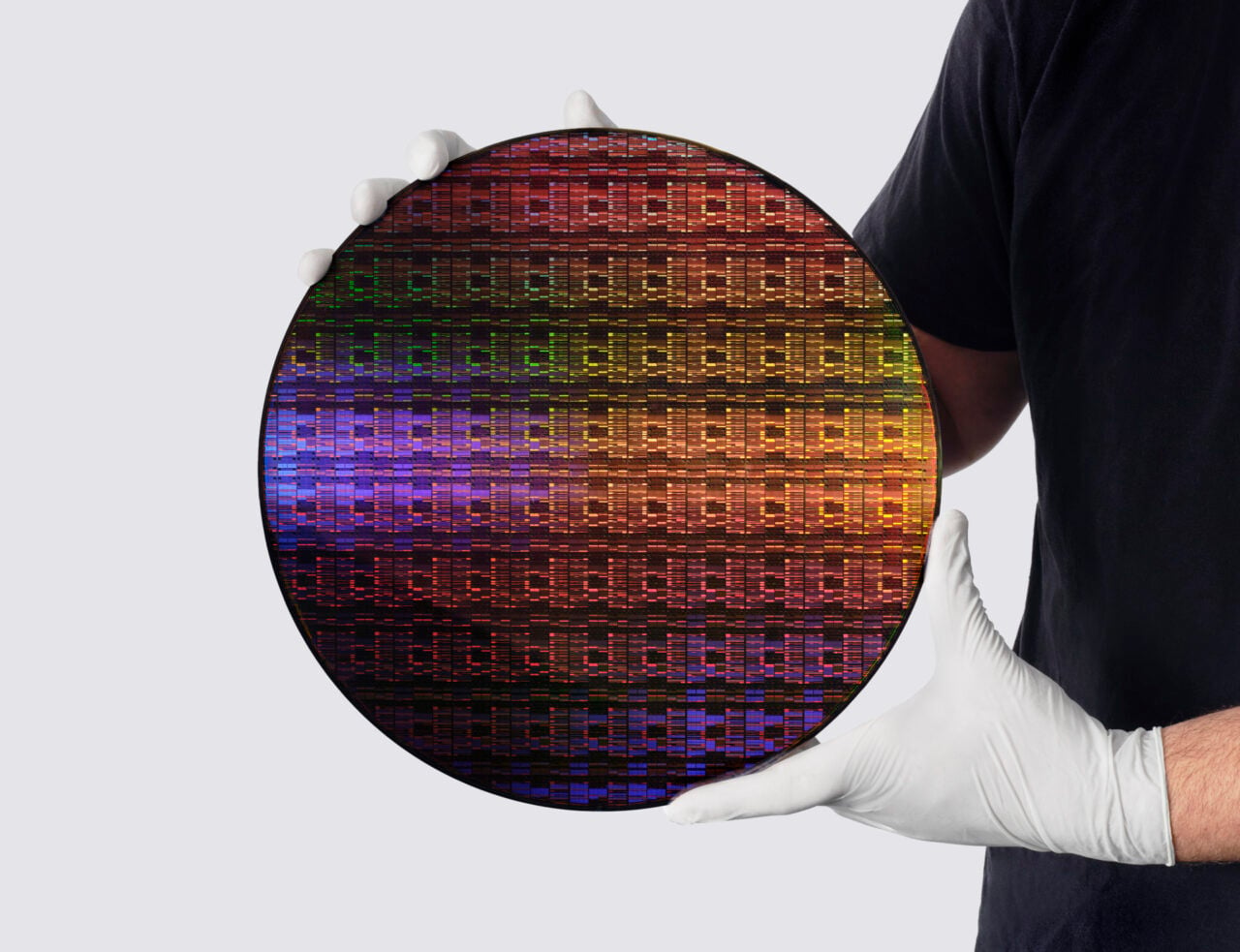
Reaching atomic levels In that sense, IBM’s latest chip represents an inventive approach for bypassing the limits of physical scaling. Specifically, two wafers with nanosheet-style transistors are glued together like a sandwich to vertically stack two layers of transistors, and related technical assessments suggested that the wafer stacking was flexible and scalable enough to support real computation, Huiming Bu, vice president of IBM’s silicon technology research team, said in a press briefing on the chip. Researcher holding IBM’s sub-1 nm node wafer. Credit: IBM That said, this chip isn’t quite ready for manufacturing just yet. The company’s goal is to enter production in the next five years, but there’s still work to be done. For instance, Bu pointed out that the team was still working on pathways to prevent thermal noise or integration into existing systems in the high-performance computing community. “From my perspective, I hope to see it be as successful as the 2-nanometer [chip] and become the industry platform,” Gambetta said during the briefing. “And as we see with AI and classical computing in general, we are only seeing more and more consumption.” #IBM #Crosses #Computings #Biggest #Barriers #Worlds #Sub1 #Nanometer #ChipIBM,Semiconductors,transistors](https://gizmodo.com/app/uploads/2026/06/nanostacking-ibm-sub-nm-chip-1280x720.jpg "IBM Crosses One of Computing’s Biggest Barriers With World’s First Sub-1 Nanometer Chip
In a major breakthrough, IBM revealed the world’s first semiconductor chip technology built on a sub-1 nanometer chipmaking process. For comparison, the process uses transistor features smaller than the width of a DNA strand, which measures about 2.5 nanometers across. The chip itself is about the size of a fingernail but holds almost 100 billion transistors, and the company expects it could enter markets as early as the next five years. In a statement released today, IBM said the new chip features nearly twice the density of its 2-nanometer chip, released in 2021. According to an accompanying technical report, the chip also demonstrated up to 70% greater energy efficiency than its predecessor. In designing the chip, researchers developed an “entirely new transistor architecture” called nanostack, which “vertically stacks and staggers transistors” to enable IBM’s 0.7-nanometer chip technology, IBM explained. A section of the chip seen with a transmission electron microscope. Credit: IBM “With our new nanostack architecture, we’re not just making smaller transistors,” Jay Gambetta, director of IBM Research, said in the statement. “We’re reinventing how chips are built to deliver dramatically more power and energy efficiency.”
Smaller and smaller Semiconductor chips enable things like computers, home appliances, communications, and transportation devices. In 1965, Intel co-founder Gordon Moore surmised that transistor capacities evolved at a predictable and consistent rate. Specifically, all things considered, the number of transistors on a semiconductor chip would double about every two years. For a while, the so-called Moore’s Law held rather well—until, that is, things hit a literal wall.
“Moore’s Law was never meant to last forever,” according to a blog post by the Massachusetts Institute of Technology’s (MIT) Computer Science and Artificial Intelligence Lab. “Transistors can only get so small and, eventually, the more permanent laws of physics get in the way.” That is, as companies try to cram more transistors into smaller chips, new advances in transistor technology take longer than two years, so Moore’s Law has been over since at least 2016, Charles Leiserson, a computer scientist at MIT, said in the blog. Accordingly, the issue now is to consider how improvements in chip performance fit into a longer-term picture, Willy Shih, an economist at Harvard Business School, said in an explainer.
Reaching atomic levels In that sense, IBM’s latest chip represents an inventive approach for bypassing the limits of physical scaling. Specifically, two wafers with nanosheet-style transistors are glued together like a sandwich to vertically stack two layers of transistors, and related technical assessments suggested that the wafer stacking was flexible and scalable enough to support real computation, Huiming Bu, vice president of IBM’s silicon technology research team, said in a press briefing on the chip. Researcher holding IBM’s sub-1 nm node wafer. Credit: IBM That said, this chip isn’t quite ready for manufacturing just yet. The company’s goal is to enter production in the next five years, but there’s still work to be done. For instance, Bu pointed out that the team was still working on pathways to prevent thermal noise or integration into existing systems in the high-performance computing community. “From my perspective, I hope to see it be as successful as the 2-nanometer [chip] and become the industry platform,” Gambetta said during the briefing. “And as we see with AI and classical computing in general, we are only seeing more and more consumption.” #IBM #Crosses #Computings #Biggest #Barriers #Worlds #Sub1 #Nanometer #ChipIBM,Semiconductors,transistors")
![IBM Crosses One of Computing’s Biggest Barriers With World’s First Sub-1 Nanometer Chip
In a major breakthrough, IBM revealed the world’s first semiconductor chip technology built on a sub-1 nanometer chipmaking process. For comparison, the process uses transistor features smaller than the width of a DNA strand, which measures about 2.5 nanometers across. The chip itself is about the size of a fingernail but holds almost 100 billion transistors, and the company expects it could enter markets as early as the next five years. In a statement released today, IBM said the new chip features nearly twice the density of its 2-nanometer chip, released in 2021. According to an accompanying technical report, the chip also demonstrated up to 70% greater energy efficiency than its predecessor. In designing the chip, researchers developed an “entirely new transistor architecture” called nanostack, which “vertically stacks and staggers transistors” to enable IBM’s 0.7-nanometer chip technology, IBM explained. A section of the chip seen with a transmission electron microscope. Credit: IBM “With our new nanostack architecture, we’re not just making smaller transistors,” Jay Gambetta, director of IBM Research, said in the statement. “We’re reinventing how chips are built to deliver dramatically more power and energy efficiency.”
Smaller and smaller Semiconductor chips enable things like computers, home appliances, communications, and transportation devices. In 1965, Intel co-founder Gordon Moore surmised that transistor capacities evolved at a predictable and consistent rate. Specifically, all things considered, the number of transistors on a semiconductor chip would double about every two years. For a while, the so-called Moore’s Law held rather well—until, that is, things hit a literal wall.
“Moore’s Law was never meant to last forever,” according to a blog post by the Massachusetts Institute of Technology’s (MIT) Computer Science and Artificial Intelligence Lab. “Transistors can only get so small and, eventually, the more permanent laws of physics get in the way.” That is, as companies try to cram more transistors into smaller chips, new advances in transistor technology take longer than two years, so Moore’s Law has been over since at least 2016, Charles Leiserson, a computer scientist at MIT, said in the blog. Accordingly, the issue now is to consider how improvements in chip performance fit into a longer-term picture, Willy Shih, an economist at Harvard Business School, said in an explainer.
Reaching atomic levels In that sense, IBM’s latest chip represents an inventive approach for bypassing the limits of physical scaling. Specifically, two wafers with nanosheet-style transistors are glued together like a sandwich to vertically stack two layers of transistors, and related technical assessments suggested that the wafer stacking was flexible and scalable enough to support real computation, Huiming Bu, vice president of IBM’s silicon technology research team, said in a press briefing on the chip. Researcher holding IBM’s sub-1 nm node wafer. Credit: IBM That said, this chip isn’t quite ready for manufacturing just yet. The company’s goal is to enter production in the next five years, but there’s still work to be done. For instance, Bu pointed out that the team was still working on pathways to prevent thermal noise or integration into existing systems in the high-performance computing community. “From my perspective, I hope to see it be as successful as the 2-nanometer [chip] and become the industry platform,” Gambetta said during the briefing. “And as we see with AI and classical computing in general, we are only seeing more and more consumption.” #IBM #Crosses #Computings #Biggest #Barriers #Worlds #Sub1 #Nanometer #ChipIBM,Semiconductors,transistors](https://i1.wp.com/gizmodo.com/app/uploads/2026/06/nanostacking-ibm-sub-nm-chip-1280x720.jpg?ssl=1 "IBM Crosses One of Computing’s Biggest Barriers With World’s First Sub-1 Nanometer Chip
In a major breakthrough, IBM revealed the world’s first semiconductor chip technology built on a sub-1 nanometer chipmaking process. For comparison, the process uses transistor features smaller than the width of a DNA strand, which measures about 2.5 nanometers across. The chip itself is about the size of a fingernail but holds almost 100 billion transistors, and the company expects it could enter markets as early as the next five years. In a statement released today, IBM said the new chip features nearly twice the density of its 2-nanometer chip, released in 2021. According to an accompanying technical report, the chip also demonstrated up to 70% greater energy efficiency than its predecessor. In designing the chip, researchers developed an “entirely new transistor architecture” called nanostack, which “vertically stacks and staggers transistors” to enable IBM’s 0.7-nanometer chip technology, IBM explained. A section of the chip seen with a transmission electron microscope. Credit: IBM “With our new nanostack architecture, we’re not just making smaller transistors,” Jay Gambetta, director of IBM Research, said in the statement. “We’re reinventing how chips are built to deliver dramatically more power and energy efficiency.”
Smaller and smaller Semiconductor chips enable things like computers, home appliances, communications, and transportation devices. In 1965, Intel co-founder Gordon Moore surmised that transistor capacities evolved at a predictable and consistent rate. Specifically, all things considered, the number of transistors on a semiconductor chip would double about every two years. For a while, the so-called Moore’s Law held rather well—until, that is, things hit a literal wall.
“Moore’s Law was never meant to last forever,” according to a blog post by the Massachusetts Institute of Technology’s (MIT) Computer Science and Artificial Intelligence Lab. “Transistors can only get so small and, eventually, the more permanent laws of physics get in the way.” That is, as companies try to cram more transistors into smaller chips, new advances in transistor technology take longer than two years, so Moore’s Law has been over since at least 2016, Charles Leiserson, a computer scientist at MIT, said in the blog. Accordingly, the issue now is to consider how improvements in chip performance fit into a longer-term picture, Willy Shih, an economist at Harvard Business School, said in an explainer.
Reaching atomic levels In that sense, IBM’s latest chip represents an inventive approach for bypassing the limits of physical scaling. Specifically, two wafers with nanosheet-style transistors are glued together like a sandwich to vertically stack two layers of transistors, and related technical assessments suggested that the wafer stacking was flexible and scalable enough to support real computation, Huiming Bu, vice president of IBM’s silicon technology research team, said in a press briefing on the chip. Researcher holding IBM’s sub-1 nm node wafer. Credit: IBM That said, this chip isn’t quite ready for manufacturing just yet. The company’s goal is to enter production in the next five years, but there’s still work to be done. For instance, Bu pointed out that the team was still working on pathways to prevent thermal noise or integration into existing systems in the high-performance computing community. “From my perspective, I hope to see it be as successful as the 2-nanometer [chip] and become the industry platform,” Gambetta said during the briefing. “And as we see with AI and classical computing in general, we are only seeing more and more consumption.” #IBM #Crosses #Computings #Biggest #Barriers #Worlds #Sub1 #Nanometer #ChipIBM,Semiconductors,transistors")
Post Comment