.jpg?ssl=1 "OpenAI Is Preparing to Launch a Social App for AI-Generated Videos")
OpenAI is preparing to launch a stand-alone app for its video generation AI model Sora 2, WIRED has learned. The app, which features a vertical video feed with swipe-to-scroll navigation, appears to closely resemble TikTok—except all of the content is AI-generated. There’s a For You–style page powered by a recommendation algorithm. On the right side of the feed, a menu bar gives users the option to like, comment, or remix a video.
Users can create videoclips up to 10 seconds long using OpenAI’s next-generation video model, according to documents viewed by WIRED. There is no option to upload photos or videos from a user’s camera roll or other apps.
The Sora 2 App has an identity verification feature that allows users to confirm their likeness. If a user has verified their identity, they can use their likeness in videos. Other users can also tag them and use their likeness in clips. For example, someone could generate a video of themselves riding a roller coaster at a theme park with a friend. Users will get a notification whenever their likeness is used—even if the clip remains in draft form and is never posted, sources say.
OpenAI launched the app internally last week. So far, it’s received overwhelmingly positive feedback from employees, according to documents viewed by WIRED. Employees have been using the tool so frequently that some managers have joked it could become a drain on productivity.
OpenAI declined to comment.
OpenAI appears to be betting that the Sora 2 app will let people interact with AI-generated video in a way that fundamentally changes their experience of the technology—similar to how ChatGPT helped users realize the potential of AI-generated text. Internally, sources say, there’s also a feeling that President Trump’s on-again, off-again deal to sell TikTok’s US operations has given OpenAI a unique opportunity to launch a short-form video app—particularly one without close ties to China.
OpenAI officially launched Sora in December of last year. Initially, people could only access it via a web page, but it was soon incorporated directly into the ChatGPT app. At the time, the model was among the most state-of-the-art AI video generators, though OpenAI noted it had some limitations. For example, it didn’t seem to fully understand physics and struggled to produce realistic action scenes, especially in longer clips.
OpenAI’s Sora 2 app will compete with new AI video offerings from tech giants like Meta and Google. Last week, Meta introduced a new feed in its Meta AI app called Vibes, which is dedicated exclusively to creating and sharing short AI-generated videos. Earlier this month, Google announced that it was integrating a custom version of its latest video generation model, Veo 3, into YouTube.
TikTok, on the other hand, has taken a more cautious approach to AI-generated content. The video app recently redefined its rules around what kind of AI-generated videos it allows on the platform. It now explicitly bans AI-generated content that’s “misleading about matters of public importance or harmful to individuals.”
Oftentimes, the Sora 2 app refuses to generate videos due to copyright safeguards and other filters, sources say. OpenAI is currently fighting a series of lawsuits over alleged copyright infringements, including a high-profile case brought by The New York Times. The Times case centers on allegations that OpenAI trained its models on the paper’s copyrighted material.
OpenAI is also facing mounting criticism over child safety issues. On Monday, the company released new parental controls, including the option for parents and teenagers to link their accounts. The company also said that it is working on an age-prediction tool that could automatically route users believed to be under the age of 18 to a more restricted version of ChatGPT that doesn’t allow for romantic interactions, among other things. It is not known what age restrictions might be incorporated into the Sora 2 app.
This is an edition of the Model Behavior newsletter. Read previous newsletters here.
Source link
#OpenAI #Preparing #Launch #Social #App #AIGenerated #Videos
![IBM Crosses One of Computing’s Biggest Barriers With World’s First Sub-1 Nanometer Chip
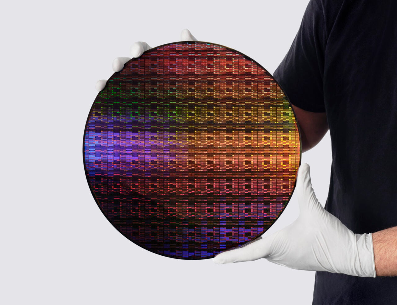
In a major breakthrough, IBM revealed the world’s first semiconductor chip technology built on a sub-1 nanometer chipmaking process. For comparison, the process uses transistor features smaller than the width of a DNA strand, which measures about 2.5 nanometers across. The chip itself is about the size of a fingernail but holds almost 100 billion transistors, and the company expects it could enter markets as early as the next five years. In a statement released today, IBM said the new chip features nearly twice the density of its 2-nanometer chip, released in 2021. According to an accompanying technical report, the chip also demonstrated up to 70% greater energy efficiency than its predecessor. In designing the chip, researchers developed an “entirely new transistor architecture” called nanostack, which “vertically stacks and staggers transistors” to enable IBM’s 0.7-nanometer chip technology, IBM explained. A section of the chip seen with a transmission electron microscope. Credit: IBM “With our new nanostack architecture, we’re not just making smaller transistors,” Jay Gambetta, director of IBM Research, said in the statement. “We’re reinventing how chips are built to deliver dramatically more power and energy efficiency.”
Smaller and smaller Semiconductor chips enable things like computers, home appliances, communications, and transportation devices. In 1965, Intel co-founder Gordon Moore surmised that transistor capacities evolved at a predictable and consistent rate. Specifically, all things considered, the number of transistors on a semiconductor chip would double about every two years. For a while, the so-called Moore’s Law held rather well—until, that is, things hit a literal wall.
“Moore’s Law was never meant to last forever,” according to a blog post by the Massachusetts Institute of Technology’s (MIT) Computer Science and Artificial Intelligence Lab. “Transistors can only get so small and, eventually, the more permanent laws of physics get in the way.” That is, as companies try to cram more transistors into smaller chips, new advances in transistor technology take longer than two years, so Moore’s Law has been over since at least 2016, Charles Leiserson, a computer scientist at MIT, said in the blog. Accordingly, the issue now is to consider how improvements in chip performance fit into a longer-term picture, Willy Shih, an economist at Harvard Business School, said in an explainer.
Reaching atomic levels In that sense, IBM’s latest chip represents an inventive approach for bypassing the limits of physical scaling. Specifically, two wafers with nanosheet-style transistors are glued together like a sandwich to vertically stack two layers of transistors, and related technical assessments suggested that the wafer stacking was flexible and scalable enough to support real computation, Huiming Bu, vice president of IBM’s silicon technology research team, said in a press briefing on the chip. Researcher holding IBM’s sub-1 nm node wafer. Credit: IBM That said, this chip isn’t quite ready for manufacturing just yet. The company’s goal is to enter production in the next five years, but there’s still work to be done. For instance, Bu pointed out that the team was still working on pathways to prevent thermal noise or integration into existing systems in the high-performance computing community. “From my perspective, I hope to see it be as successful as the 2-nanometer [chip] and become the industry platform,” Gambetta said during the briefing. “And as we see with AI and classical computing in general, we are only seeing more and more consumption.” #IBM #Crosses #Computings #Biggest #Barriers #Worlds #Sub1 #Nanometer #ChipIBM,Semiconductors,transistors](https://gizmodo.com/app/uploads/2026/06/nanostacking-ibm-sub-nm-chip-1280x720.jpg "IBM Crosses One of Computing’s Biggest Barriers With World’s First Sub-1 Nanometer Chip
In a major breakthrough, IBM revealed the world’s first semiconductor chip technology built on a sub-1 nanometer chipmaking process. For comparison, the process uses transistor features smaller than the width of a DNA strand, which measures about 2.5 nanometers across. The chip itself is about the size of a fingernail but holds almost 100 billion transistors, and the company expects it could enter markets as early as the next five years. In a statement released today, IBM said the new chip features nearly twice the density of its 2-nanometer chip, released in 2021. According to an accompanying technical report, the chip also demonstrated up to 70% greater energy efficiency than its predecessor. In designing the chip, researchers developed an “entirely new transistor architecture” called nanostack, which “vertically stacks and staggers transistors” to enable IBM’s 0.7-nanometer chip technology, IBM explained. A section of the chip seen with a transmission electron microscope. Credit: IBM “With our new nanostack architecture, we’re not just making smaller transistors,” Jay Gambetta, director of IBM Research, said in the statement. “We’re reinventing how chips are built to deliver dramatically more power and energy efficiency.”
Smaller and smaller Semiconductor chips enable things like computers, home appliances, communications, and transportation devices. In 1965, Intel co-founder Gordon Moore surmised that transistor capacities evolved at a predictable and consistent rate. Specifically, all things considered, the number of transistors on a semiconductor chip would double about every two years. For a while, the so-called Moore’s Law held rather well—until, that is, things hit a literal wall.
“Moore’s Law was never meant to last forever,” according to a blog post by the Massachusetts Institute of Technology’s (MIT) Computer Science and Artificial Intelligence Lab. “Transistors can only get so small and, eventually, the more permanent laws of physics get in the way.” That is, as companies try to cram more transistors into smaller chips, new advances in transistor technology take longer than two years, so Moore’s Law has been over since at least 2016, Charles Leiserson, a computer scientist at MIT, said in the blog. Accordingly, the issue now is to consider how improvements in chip performance fit into a longer-term picture, Willy Shih, an economist at Harvard Business School, said in an explainer.
Reaching atomic levels In that sense, IBM’s latest chip represents an inventive approach for bypassing the limits of physical scaling. Specifically, two wafers with nanosheet-style transistors are glued together like a sandwich to vertically stack two layers of transistors, and related technical assessments suggested that the wafer stacking was flexible and scalable enough to support real computation, Huiming Bu, vice president of IBM’s silicon technology research team, said in a press briefing on the chip. Researcher holding IBM’s sub-1 nm node wafer. Credit: IBM That said, this chip isn’t quite ready for manufacturing just yet. The company’s goal is to enter production in the next five years, but there’s still work to be done. For instance, Bu pointed out that the team was still working on pathways to prevent thermal noise or integration into existing systems in the high-performance computing community. “From my perspective, I hope to see it be as successful as the 2-nanometer [chip] and become the industry platform,” Gambetta said during the briefing. “And as we see with AI and classical computing in general, we are only seeing more and more consumption.” #IBM #Crosses #Computings #Biggest #Barriers #Worlds #Sub1 #Nanometer #ChipIBM,Semiconductors,transistors")
![IBM Crosses One of Computing’s Biggest Barriers With World’s First Sub-1 Nanometer Chip
In a major breakthrough, IBM revealed the world’s first semiconductor chip technology built on a sub-1 nanometer chipmaking process. For comparison, the process uses transistor features smaller than the width of a DNA strand, which measures about 2.5 nanometers across. The chip itself is about the size of a fingernail but holds almost 100 billion transistors, and the company expects it could enter markets as early as the next five years. In a statement released today, IBM said the new chip features nearly twice the density of its 2-nanometer chip, released in 2021. According to an accompanying technical report, the chip also demonstrated up to 70% greater energy efficiency than its predecessor. In designing the chip, researchers developed an “entirely new transistor architecture” called nanostack, which “vertically stacks and staggers transistors” to enable IBM’s 0.7-nanometer chip technology, IBM explained. A section of the chip seen with a transmission electron microscope. Credit: IBM “With our new nanostack architecture, we’re not just making smaller transistors,” Jay Gambetta, director of IBM Research, said in the statement. “We’re reinventing how chips are built to deliver dramatically more power and energy efficiency.”
Smaller and smaller Semiconductor chips enable things like computers, home appliances, communications, and transportation devices. In 1965, Intel co-founder Gordon Moore surmised that transistor capacities evolved at a predictable and consistent rate. Specifically, all things considered, the number of transistors on a semiconductor chip would double about every two years. For a while, the so-called Moore’s Law held rather well—until, that is, things hit a literal wall.
“Moore’s Law was never meant to last forever,” according to a blog post by the Massachusetts Institute of Technology’s (MIT) Computer Science and Artificial Intelligence Lab. “Transistors can only get so small and, eventually, the more permanent laws of physics get in the way.” That is, as companies try to cram more transistors into smaller chips, new advances in transistor technology take longer than two years, so Moore’s Law has been over since at least 2016, Charles Leiserson, a computer scientist at MIT, said in the blog. Accordingly, the issue now is to consider how improvements in chip performance fit into a longer-term picture, Willy Shih, an economist at Harvard Business School, said in an explainer.
Reaching atomic levels In that sense, IBM’s latest chip represents an inventive approach for bypassing the limits of physical scaling. Specifically, two wafers with nanosheet-style transistors are glued together like a sandwich to vertically stack two layers of transistors, and related technical assessments suggested that the wafer stacking was flexible and scalable enough to support real computation, Huiming Bu, vice president of IBM’s silicon technology research team, said in a press briefing on the chip. Researcher holding IBM’s sub-1 nm node wafer. Credit: IBM That said, this chip isn’t quite ready for manufacturing just yet. The company’s goal is to enter production in the next five years, but there’s still work to be done. For instance, Bu pointed out that the team was still working on pathways to prevent thermal noise or integration into existing systems in the high-performance computing community. “From my perspective, I hope to see it be as successful as the 2-nanometer [chip] and become the industry platform,” Gambetta said during the briefing. “And as we see with AI and classical computing in general, we are only seeing more and more consumption.” #IBM #Crosses #Computings #Biggest #Barriers #Worlds #Sub1 #Nanometer #ChipIBM,Semiconductors,transistors](https://i1.wp.com/gizmodo.com/app/uploads/2026/06/nanostacking-ibm-sub-nm-chip-1280x720.jpg?ssl=1 "IBM Crosses One of Computing’s Biggest Barriers With World’s First Sub-1 Nanometer Chip
In a major breakthrough, IBM revealed the world’s first semiconductor chip technology built on a sub-1 nanometer chipmaking process. For comparison, the process uses transistor features smaller than the width of a DNA strand, which measures about 2.5 nanometers across. The chip itself is about the size of a fingernail but holds almost 100 billion transistors, and the company expects it could enter markets as early as the next five years. In a statement released today, IBM said the new chip features nearly twice the density of its 2-nanometer chip, released in 2021. According to an accompanying technical report, the chip also demonstrated up to 70% greater energy efficiency than its predecessor. In designing the chip, researchers developed an “entirely new transistor architecture” called nanostack, which “vertically stacks and staggers transistors” to enable IBM’s 0.7-nanometer chip technology, IBM explained. A section of the chip seen with a transmission electron microscope. Credit: IBM “With our new nanostack architecture, we’re not just making smaller transistors,” Jay Gambetta, director of IBM Research, said in the statement. “We’re reinventing how chips are built to deliver dramatically more power and energy efficiency.”
Smaller and smaller Semiconductor chips enable things like computers, home appliances, communications, and transportation devices. In 1965, Intel co-founder Gordon Moore surmised that transistor capacities evolved at a predictable and consistent rate. Specifically, all things considered, the number of transistors on a semiconductor chip would double about every two years. For a while, the so-called Moore’s Law held rather well—until, that is, things hit a literal wall.
“Moore’s Law was never meant to last forever,” according to a blog post by the Massachusetts Institute of Technology’s (MIT) Computer Science and Artificial Intelligence Lab. “Transistors can only get so small and, eventually, the more permanent laws of physics get in the way.” That is, as companies try to cram more transistors into smaller chips, new advances in transistor technology take longer than two years, so Moore’s Law has been over since at least 2016, Charles Leiserson, a computer scientist at MIT, said in the blog. Accordingly, the issue now is to consider how improvements in chip performance fit into a longer-term picture, Willy Shih, an economist at Harvard Business School, said in an explainer.
Reaching atomic levels In that sense, IBM’s latest chip represents an inventive approach for bypassing the limits of physical scaling. Specifically, two wafers with nanosheet-style transistors are glued together like a sandwich to vertically stack two layers of transistors, and related technical assessments suggested that the wafer stacking was flexible and scalable enough to support real computation, Huiming Bu, vice president of IBM’s silicon technology research team, said in a press briefing on the chip. Researcher holding IBM’s sub-1 nm node wafer. Credit: IBM That said, this chip isn’t quite ready for manufacturing just yet. The company’s goal is to enter production in the next five years, but there’s still work to be done. For instance, Bu pointed out that the team was still working on pathways to prevent thermal noise or integration into existing systems in the high-performance computing community. “From my perspective, I hope to see it be as successful as the 2-nanometer [chip] and become the industry platform,” Gambetta said during the briefing. “And as we see with AI and classical computing in general, we are only seeing more and more consumption.” #IBM #Crosses #Computings #Biggest #Barriers #Worlds #Sub1 #Nanometer #ChipIBM,Semiconductors,transistors")


-SOURCE-Scott-Gilbertson.jpg)
-SOURCE-Scott-Gilbertson.jpg)
-SOURCE-Scott-Gilbertson.jpg)
 is my favorite 360 camera. The dual 14-mm (35-mm equivalent) lenses of the Max 2 each record up to a 1/2.3-inch chip, yielding what GoPro calls “True 8K” (10-bit) video. The larger sensors of the Max 2 provide sharper, clearer footage than other 360 cameras, and you can record 10-bit color in log for greater flexibility in post-production color grading—a capability you’d be hard-pressed to find in other 360 cameras. Even if editing log footage is too much work (I hear you), GoPro’s natural-looking color rendition in the default color profile is still the best I’ve tested.As with most GoPros, the Max 2 has three mounting options: folding fingers, a tripod hole, and a magnetic system. This means you can mount the Max 2 just about anywhere. It also has the simplest lens-cover replacement process. To do it, just twist off the lenses with your fingers and pop on the new ones. You’ll get all the usual GoPro video modes, including HyperSmooth video stabilization, horizon leveling, TimeWarp, and more.The one flaw in the Max 2 is its lackluster audio quality. The best way to avoid that issue is to pair the camera with a Bluetooth mic. Also note that if low-light video is on your list of must-haves in an action camera, the Insta360 X5 (below) is probably a better bet. For everyone else, though, this is the 360 camera to get—especially at this discounted price.The Best Action Camera for VloggingPhotograph: Scott GilbertsonPhotograph: Scott GilbertsonPhotograph: Scott GilbertsonThe Insta360 Ace Pro 2 (8/10 WIRED Recommends) combines a great Leica lens with an 8K-capable sensor and a handy flip-up rear screen, which is why it’s my favorite action camera for vlogging. The 8K video is not that great for action footage, but the camera is nice for slower shots, which you can crop and still export to 4K. The standout feature, though, is the rear screen. Other action cameras offer a small front screen to compose selfies, but the Ace Pro 2’s entire huge rear screen is there to help you frame yourself. The rear screen also simplifies shooting from the hip and nailing other unusual angles, especially when paired with the Xplorer Grip Pro ( off).#GoPro #Deals #Good #Youll #Jump #Cliffamazon prime day,cameras,gopro,shopping,deals,buying guides,amazon prime day deals")
 Amazon’s inventory is starting to dwindle as we approach the midway point of Prime Day, but Walmart still has a few colorways in stock at the same price; it’s running a sale of its own this week.
SEE ALSO:
Amazon Prime Day is here: We found 75+ deals on Apple, Sony, Kindle, and Lego favorites
Meanwhile, the entry-level AirPods 4 and noise-cancelling AirPods Pro 3 are both on sale for up to off this Prime Day. Neither model is matching its biggest discount on record, but given Apple’s plans for price hikes in the near future, these are probably going to be their best deals for a while.Read on for our rundown of the best Prime Day AirPods deals available. If you’re a brand loyalist, be sure to check out our dedicated guide to the top Prime Day deals on all Apple products. Best AirPods deal
at Amazon
9
Save
Why we like itThe vanilla AirPods 4 are our No. 1 Apple earbuds for budget buyers. In our testing, they sounded fantastic, fit comfortably, and worked seamlessly with other Apple devices. We saw them drop all the way down to last Black Friday, but is their best price so far in 2026. Save at Amazon and Walmart. (PSA: Walmart also has pre-owned AirPods 4 on sale for just .)The AirPods 4 are also available with ANC. That pair is on sale for 8.99 (normally 9) at Amazon, Walmart, and Costco. For reference, their record-low price is .Read Mashable’s full review of the AirPods 4 with ANC.Best AirPods Pro deal
9
at Amazon
9
Save
The AirPods Pro 3 are our favorite AirPods across all price points, offering great ANC, an eight-hour battery life, plus extra fixings like a built-in heart rate monitor. They’re also more water- and sweat-resistant than the regular AirPods 4, making them better for working out. They were only 9 on Amazon last week, but at the time of writing, they were sitting at 9 there. Walmart was price-matching them.Read Mashable’s full review of the AirPods Pro 3.
Mashable Deals
By signing up, you agree to receive recurring automated SMS marketing messages from Mashable Deals at the number provided. Msg and data rates may apply. Up to 2 messages/day. Reply STOP to opt out, HELP for help. Consent is not a condition of purchase. See our Privacy Policy and Terms of Use.
Best AirPods Max deal
9
at Amazon
9
Save 0
Apple’s newly updated headphones have better ANC than the original AirPods Max from 2021. They run on the same H2 chip as the AirPods Pro 3, so they support the same software features (such as Live Translation and Conversation Awareness). In one of the best and most unexpected Prime Day deals thus far, they’re on sale for just 9 this week — a new all-time low. Amazon had them in stock at that price in midnight at the time of writing. They’re price-matched at Walmart in blue, purple, and starlight.Read Mashable’s full review of the AirPods Max 2.We will be regularly updating this guide with the best Prime Day AirPods deals, so keep checking back. You can also visit our Prime Day 2026 hub for all the latest updates and price drops.
#Prime #Day #AirPods #deals #AirPods #Max #recordlow #price")
Post Comment